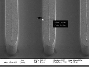
Specific Process Knowledge/Etch/Etching of Silicon Oxide/SiO2 etch using RIE1 or RIE2/Images of 1SIO2mbr with burned resist mask: Difference between revisions
Jump to navigation
Jump to search
No edit summary |
|||
| (One intermediate revision by one other user not shown) | |||
| Line 1: | Line 1: | ||
'''Feedback to this page''': '''[mailto:labadviser@ | '''Feedback to this page''': '''[mailto:labadviser@nanolab.dtu.dk?Subject=Feed%20back%20from%20page%20http://labadviser.nanolab.dtu.dk/index.php/Specific_Process_Knowledge/Etch/Etching_of_Silicon_Oxide/SiO2_etch_using_RIE1_or_RIE2/Images_of_1SIO2mbr_with_burned_resist_mask click here]''' | ||
=<span style="color:#FF0000"> Both RIE's (RIE1 and RIE2) for silicon based etching has been decommissioned </span> = | =<span style="color:#FF0000"> Both RIE's (RIE1 and RIE2) for silicon based etching has been decommissioned </span> = | ||
* <span style="color:#FF0000"> This information is save because it might be valuable as inspiration for other dry etch systems. | |||
===Etch of SiO2 using the recipe 1SIO2mbr with burned resist as masking material === | ===Etch of SiO2 using the recipe 1SIO2mbr with burned resist as masking material === | ||
''Berit Geilman Herstrøm (BGE) from | ''Berit Geilman Herstrøm (BGE) from Nanolab@DTU'' | ||
{| border="2" cellspacing="1" cellpadding="3" align="left" | {| border="2" cellspacing="1" cellpadding="3" align="left" | ||
Latest revision as of 13:07, 6 September 2022
Feedback to this page: click here
Both RIE's (RIE1 and RIE2) for silicon based etching has been decommissioned
- This information is save because it might be valuable as inspiration for other dry etch systems.
Etch of SiO2 using the recipe 1SIO2mbr with burned resist as masking material
Berit Geilman Herstrøm (BGE) from Nanolab@DTU
