Specific Process Knowledge/Thin film deposition/Deposition of Silicon/Si sputter in Sputter-System Metal-Oxide(PC3): Difference between revisions
No edit summary |
|||
| Line 1: | Line 1: | ||
This page presents the results of Si deposition using <b>RF</b> and <b>Pulsed-DC Sputtering</b> in Sputter-System Metal-Nitride (PC3) commonly known as "Cluster Lesker". The deposition target is 4" <b>Si</b>. Source #1 was used. Materials from this source can either be deposited with RF or p-DC sputtering. Here, the results from both methods will be covered. | |||
The deposition and characterization described below were conducted in <b>2022 by Evgeniy Shkondin, DTU Nanolab</b>. The main focus of the study was the deposition rate, optical functions, and the general performance of deposition from a bigger 4” target. The silicon sputtering from the target of this size allows achieving a higher deposition rate and service to many potential applications where several hundreds of nm are needed to be put uniformly on a wafer of 150mm or similar. Besides, it offers the additional possibility to deposit Si using Cluster Lesker in case another chamber (PC1) where the Si process is also established fails for some reason. | The deposition and characterization described below were conducted in <b>2022 by Evgeniy Shkondin, DTU Nanolab</b>. The main focus of the study was the deposition rate, optical functions, and the general performance of deposition from a bigger 4” target. The silicon sputtering from the target of this size allows achieving a higher deposition rate and service to many potential applications where several hundreds of nm are needed to be put uniformly on a wafer of 150mm or similar. Besides, it offers the additional possibility to deposit Si using Cluster Lesker in case another chamber (PC1) where the Si process is also established fails for some reason. | ||
| Line 13: | Line 11: | ||
=RF Sputtering of Si in Sputter-System Metal-Nitride(PC3)= | |||
The RF Si process recipe in a Sputter-System Metal-Nitride(PC3) is following: | |||
* Recipe Name: <b>MD PC3_Src1 - RF_Upstream</b> | |||
* PC Gun Z-shift Position: Home (00.00 mm) and Extended (95.20 mm) | * PC Gun Z-shift Position: Home (00.00 mm) and Extended (95.20 mm) | ||
| Line 33: | Line 35: | ||
</gallery> | </gallery> | ||
=Characterization= | ==Characterization (RF mode)== | ||
==Spectroscopic ellipsometry== | ===Spectroscopic ellipsometry (RF mode)=== | ||
Thicknesses have been measured by spectroscopic ellipsometry (VASE ellipsometer) across different locations on 6" Si wafer with 300nm dry SiO<sub>2</sub>. The optical model is based on Tauc-Lorentz and two Lorentz oscillators. The deposition parameters are present in the recipe written above. The results are present in a table below: | Thicknesses have been measured by spectroscopic ellipsometry (VASE ellipsometer) across different locations on 6" Si wafer with 300nm dry SiO<sub>2</sub>. The optical model is based on Tauc-Lorentz and two Lorentz oscillators. The deposition parameters are present in the recipe written above. The results are present in a table below: | ||
| Line 179: | Line 181: | ||
<!-- --> | <!-- --> | ||
===Deposition rate=== | ====Deposition rate (RF mode)==== | ||
<gallery caption="Effect of power on deposition rate (for two different Gun Z-shift Positions). " widths="600px" heights="500px" perrow="2"> | <gallery caption="Effect of power on deposition rate (for two different Gun Z-shift Positions). " widths="600px" heights="500px" perrow="2"> | ||
| Line 194: | Line 196: | ||
Deposition rate (nm/s) = <math> 0.0002504444 \cdot Power - 0.022223333</math> | Deposition rate (nm/s) = <math> 0.0002504444 \cdot Power - 0.022223333</math> | ||
=== Uniformity === | ==== Uniformity (RF mode) ==== | ||
<gallery caption="Uniformity of deposited Si layer across 6-inch wafer. " widths="200px" heights="200px" perrow="5"> | <gallery caption="Uniformity of deposited Si layer across 6-inch wafer. " widths="200px" heights="200px" perrow="5"> | ||
| Line 209: | Line 211: | ||
</gallery> | </gallery> | ||
=== Optical functions === | ==== Optical functions (RF mode)==== | ||
<gallery caption="Optical constants of deposited Si layer." widths="600px" heights="500px" perrow="2"> | <gallery caption="Optical constants of deposited Si layer." widths="600px" heights="500px" perrow="2"> | ||
| Line 218: | Line 220: | ||
</gallery> | </gallery> | ||
== DC Bias recordings == | === DC Bias recordings (RF mode)=== | ||
Any deposition recipe the user runs on Cluster Lesker is getting recorded. Many parameters are stored in the datalog files (in the 1-second interval) that can be accessed and viewed later. Here the DC bias was monitored for the whole experiment. | Any deposition recipe the user runs on Cluster Lesker is getting recorded. Many parameters are stored in the datalog files (in the 1-second interval) that can be accessed and viewed later. Here the DC bias was monitored for the whole experiment. | ||
| Line 225: | Line 227: | ||
image:eves_PC3_Src1_Si_RF_extended_bias_20220726.png| DC bias variation during the process for different powers (Extended gun position case). | image:eves_PC3_Src1_Si_RF_extended_bias_20220726.png| DC bias variation during the process for different powers (Extended gun position case). | ||
image:eves_PC3_Src1_Si_RF_home_bias_20220726.png| DC bias variation during the process for different powers (Home gun position case). | image:eves_PC3_Src1_Si_RF_home_bias_20220726.png| DC bias variation during the process for different powers (Home gun position case). | ||
</gallery> | |||
=Pulsed DC Sputtering of Si in Sputter-System Metal-Nitride(PC3)= | |||
This section covers the results from the pulsed DC deposition method. | |||
It must be mentioned that the lower powers give an unstable plasma and varying DC Bias voltage. This is why it is strongly recommended to run this process at the range of <b>180W-200W</b> (although not higher since the target can only withstand 20 W/cm<sup>2</sup> power density which means the maximum power of approximately 200W for a 4-inch target ). | |||
Besides, it is also challenging to ignite and maintain plasma using the pulsed-DC power supply at the very beginning of the process, where the power values are still low. It is strongly recommended to <b>ramp the power with the opened source shutter</b>. | |||
The Pulsed-DC Si process recipe in a Sputter-System Metal-Nitride(PC3) is following: | |||
* Recipe Name: <b>MD PC3_Src1 - Pulse DC_Upstream</b> | |||
* PC Gun Z-shift Position: Home (00.00 mm) and Extended (95.20 mm) | |||
* Tilt: No (Target in horizontal plane) | |||
* Deposition mode: <b>Upstream</b> | |||
* Rotation speed: <b>10 rpm</b> | |||
* Pressure: <b>3 mTorr</b> | |||
* Power: <b>120-200 W</b> (It is recomended to use <b>200W</b> for for the most stable DC bias voltage). | |||
* Frequency: <b>100 kHz</b> | |||
* Reverse time: <b>1 µs</b> | |||
* Deposition time: <b>1800s</b> | |||
* Deposition temperature: <b>room temperature</b> | |||
Samples: 6" Si with 300nm SiO<sub>2</sub> (from furnace C1 recipe: DRY1100 05:00:00 + 20 min annealing) | |||
<gallery caption="The photography of Si target mounted in 4” magnetron (PC3 Src1). " widths="400px" heights="500px" perrow="2"> | |||
image:eves_PC3_Src1_Si_Home_position_20220726.png|PC Gun Z-shift Position: Home (00.00 mm). | |||
image:eves_PC3_Src1_Si_Extended_position_20220726.png|PC Gun Z-shift Position: Extended (95.20 mm). | |||
</gallery> | |||
==Characterization (p-DC)== | |||
===Spectroscopic ellipsometry (p-DC)=== | |||
Thicknesses have been measured by spectroscopic ellipsometry (VASE ellipsometer) across different locations on 6" Si wafer with 300nm dry SiO<sub>2</sub>. The optical model is based on Tauc-Lorentz and two Lorentz oscillators. The deposition parameters are present in the recipe written above. The results are present in a table below: | |||
{| border="2" cellspacing="0" cellpadding="9" | |||
!colspan="8" border="none" style="background:WhiteSmoke; color:black;" align="center"| PC Gun Z-shift Position: Extended (95.20 mm) | |||
|- | |||
!colspan="1" border="none" style="background:silver; color:black;" align="center"|Deposition conditions | |||
Power (W) | |||
|style="background:silver; color:black"|<b>Time (s)</b> | |||
|style="background:silver; color:black"|<b>Pressure (mTorr)</b> | |||
|style="background:silver; color:black"|<b>Average (nm)</b> | |||
|style="background:silver; color:black"|<b>Standard deviation</b> | |||
|style="background:silver; color:black"|<b>Minimum Thickness (nm)</b> | |||
|style="background:silver; color:black"|<b>Maximum Thickness (nm)</b> | |||
|style="background:silver; color:black"|<b>Rate (nm/s)</b> | |||
|- | |||
!style="background:silver; color:black;" align="center" |120 W | |||
|style="background:WhiteSmoke; color:black" align="center"|1800 | |||
|style="background:WhiteSmoke; color:black" align="center"|3 | |||
|style="background:WhiteSmoke; color:black" align="center"|98.10 | |||
|style="background:WhiteSmoke; color:black" align="center"|2.99 | |||
|style="background:WhiteSmoke; color:black" align="center"|91.47 | |||
|style="background:WhiteSmoke; color:black" align="center"|101.35 | |||
|style="background:WhiteSmoke; color:black" align="center"|<b><span style="color: red">0.0545</span></b> | |||
|- | |||
!style="background:silver; color:black;" align="center" |160 W | |||
|style="background:WhiteSmoke; color:black" align="center"|1800 | |||
|style="background:WhiteSmoke; color:black" align="center"|3 | |||
|style="background:WhiteSmoke; color:black" align="center"|239.87 | |||
|style="background:WhiteSmoke; color:black" align="center"|4.26 | |||
|style="background:WhiteSmoke; color:black" align="center"|229.95 | |||
|style="background:WhiteSmoke; color:black" align="center"|244.61 | |||
|style="background:WhiteSmoke; color:black" align="center"|<b><span style="color: red">0.1333</span></b> | |||
|- | |||
!style="background:silver; color:black;" align="center" |200 W | |||
|style="background:WhiteSmoke; color:black" align="center"|1800 | |||
|style="background:WhiteSmoke; color:black" align="center"|3 | |||
|style="background:WhiteSmoke; color:black" align="center"|311.43 | |||
|style="background:WhiteSmoke; color:black" align="center"|5.38 | |||
|style="background:WhiteSmoke; color:black" align="center"|299.99 | |||
|style="background:WhiteSmoke; color:black" align="center"|316.45 | |||
|style="background:WhiteSmoke; color:black" align="center"|<b><span style="color: red">0.1730</span></b> | |||
|- | |||
|} | |||
<br> | |||
<!-- --> | |||
{| border="2" cellspacing="0" cellpadding="9" | |||
!colspan="8" border="none" style="background:WhiteSmoke; color:black;" align="center"| PC Gun Z-shift Position: Home (00.00 mm) | |||
|- | |||
!colspan="1" border="none" style="background:silver; color:black;" align="center"|Deposition conditions | |||
Power (W) | |||
|style="background:silver; color:black"|<b>Time (s)</b> | |||
|style="background:silver; color:black"|<b>Pressure (mTorr)</b> | |||
|style="background:silver; color:black"|<b>Average (nm)</b> | |||
|style="background:silver; color:black"|<b>Standard deviation</b> | |||
|style="background:silver; color:black"|<b>Minimum Thickness (nm)</b> | |||
|style="background:silver; color:black"|<b>Maximum Thickness (nm)</b> | |||
|style="background:silver; color:black"|<b>Rate (nm/s)</b> | |||
|- | |||
!style="background:silver; color:black;" align="center" |120 W | |||
|style="background:WhiteSmoke; color:black" align="center"|1800 | |||
|style="background:WhiteSmoke; color:black" align="center"|3 | |||
|style="background:WhiteSmoke; color:black" align="center"|37.49 | |||
|style="background:WhiteSmoke; color:black" align="center"|1.51 | |||
|style="background:WhiteSmoke; color:black" align="center"|34.39 | |||
|style="background:WhiteSmoke; color:black" align="center"|39.86 | |||
|style="background:WhiteSmoke; color:black" align="center"|<b><span style="color: red">0.0208</span></b> | |||
|- | |||
!style="background:silver; color:black;" align="center" |160 W | |||
|style="background:WhiteSmoke; color:black" align="center"|1800 | |||
|style="background:WhiteSmoke; color:black" align="center"|3 | |||
|style="background:WhiteSmoke; color:black" align="center"|95.83 | |||
|style="background:WhiteSmoke; color:black" align="center"|4.27 | |||
|style="background:WhiteSmoke; color:black" align="center"|89.54 | |||
|style="background:WhiteSmoke; color:black" align="center"|102.62 | |||
|style="background:WhiteSmoke; color:black" align="center"|<b><span style="color: red">0.0532</span></b> | |||
|- | |||
!style="background:silver; color:black;" align="center" |200 W | |||
|style="background:WhiteSmoke; color:black" align="center"|1800 | |||
|style="background:WhiteSmoke; color:black" align="center"|3 | |||
|style="background:WhiteSmoke; color:black" align="center"|134.73 | |||
|style="background:WhiteSmoke; color:black" align="center"|6.97 | |||
|style="background:WhiteSmoke; color:black" align="center"|123.37 | |||
|style="background:WhiteSmoke; color:black" align="center"|145.90 | |||
|style="background:WhiteSmoke; color:black" align="center"|<b><span style="color: red">0.0748</span></b> | |||
|- | |||
|} | |||
<br> | |||
<!-- --> | |||
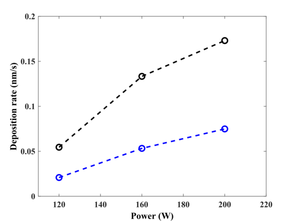
====Deposition rate (p-DC)==== | |||
<gallery caption="Effect of power on deposition rate (for two different Gun Z-shift Positions). " widths="600px" heights="500px" perrow="2"> | |||
image:eves_PC3_Src1_Si_pDC_thickness_vs_power_20220802.png| Measured thickness vs. power. | |||
image:eves_PC3_Src1_Si_pDC_deprate_vs_power_20220802.png| Deposition rate as a function of power. | |||
</gallery> | |||
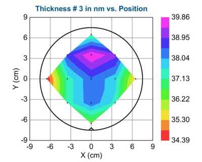
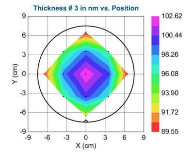
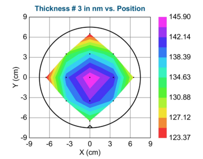
==== Uniformity (p-DC)==== | |||
<gallery caption="Uniformity of deposited Si layer across 6-inch wafer. " widths="400px" heights="400px" perrow="3"> | |||
image:eves_PC3_Src1_Si_pDC_Ext_120W_uniformity_20220802.png|120 W; PC Gun Z-shift Position: Extended (95.20 mm) | |||
image:eves_PC3_Src1_Si_pDC_Ext_160W_uniformity_20220802.png|160 W; PC Gun Z-shift Position: Extended (95.20 mm) | |||
image:eves_PC3_Src1_Si_pDC_Ext_200W_uniformity_20220802.png|200 W; PC Gun Z-shift Position: Extended (95.20 mm) | |||
image:eves_PC3_Src1_Si_pDC_Home_120W_uniformity_20220802.png|120 W; PC Gun Z-shift Position: Home (00.00 mm) | |||
image:eves_PC3_Src1_Si_pDC_Home_160W_uniformity_20220802.png|160 W; PC Gun Z-shift Position: Home (00.00 mm) | |||
image:eves_PC3_Src1_Si_pDC_Home_200W_uniformity_20220802.png|200 W; PC Gun Z-shift Position: Home (00.00 mm) | |||
</gallery> | |||
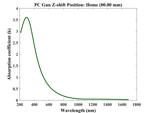
==== Optical functions (p-DC)==== | |||
<gallery caption="Optical constants of deposited Si layer." widths="600px" heights="500px" perrow="2"> | |||
image:eves_PC3_Src1_Si_pDC_refractive_index_extended_20220802.png|Refractive index (extended position). | |||
image:eves_PC3_Src1_Si_pDC_refractive_index_home_20220802.png|Refractive index (home position). | |||
image:eves_PC3_Src1_Si_pDC_absorption_coeff_extended_20220802.png|Absorption coefficient (extended position). | |||
image:eves_PC3_Src1_Si_pDC_absorption_coeff_home_20220802.png|Absorption coefficient (home position). | |||
</gallery> | |||
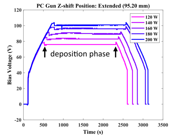
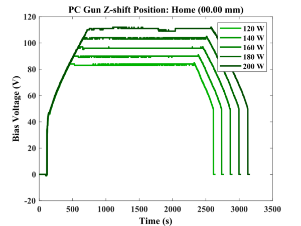
=== DC Bias recordings (p-DC)=== | |||
Any deposition recipe the user runs on Cluster Lesker is getting recorded. Many parameters are stored in the datalog files (in the 1-second interval) that can be accessed and viewed later. Here the DC bias was monitored for the whole experiment. | |||
<gallery caption="DC bias recordings. " widths="600px" heights="500px" perrow="2"> | |||
image:eves_PC3_Src1_Si_pDC_extended_bias_20220802.png| DC bias variation during the process for different powers (Extended gun position case). | |||
image:eves_PC3_Src1_Si_pDC_home_bias_20220802.png| DC bias variation during the process for different powers (Home gun position case). | |||
</gallery> | </gallery> | ||
Revision as of 17:09, 2 August 2022
This page presents the results of Si deposition using RF and Pulsed-DC Sputtering in Sputter-System Metal-Nitride (PC3) commonly known as "Cluster Lesker". The deposition target is 4" Si. Source #1 was used. Materials from this source can either be deposited with RF or p-DC sputtering. Here, the results from both methods will be covered.
The deposition and characterization described below were conducted in 2022 by Evgeniy Shkondin, DTU Nanolab. The main focus of the study was the deposition rate, optical functions, and the general performance of deposition from a bigger 4” target. The silicon sputtering from the target of this size allows achieving a higher deposition rate and service to many potential applications where several hundreds of nm are needed to be put uniformly on a wafer of 150mm or similar. Besides, it offers the additional possibility to deposit Si using Cluster Lesker in case another chamber (PC1) where the Si process is also established fails for some reason.
The depositions performed with closed dark space shield configuaration (see photography below). The dark space shield is a circular protection cylinder that sits around the cathode, in its close configuration the top part of the shield is bent toward the target and shadows a few mm of it.
It must be mentioned that the dark space shield should be in a “closed-form” only, as it was observed that the “opened” dark space shield configuration can do a side wall Cu sputtering. This will heavily contaminate the film and gradually damage the tool.
4” magnetron in PC3 has more functionalities compared to the ordinary guns in cluster Lesker. It can(to some degree) moves in Z-direction. This will affect the deposition rate, uniformity and most likely play an important role in reactive sputtering. Besides that, it can be easily tilted if necessary. In this study, two z-high positions have been compared (lowes-“home” and highest –“extended”). The effect of power has also been evaluated.
RF Sputtering of Si in Sputter-System Metal-Nitride(PC3)
The RF Si process recipe in a Sputter-System Metal-Nitride(PC3) is following:
* Recipe Name: MD PC3_Src1 - RF_Upstream
- PC Gun Z-shift Position: Home (00.00 mm) and Extended (95.20 mm)
- Tilt: No (Target in horizontal plane)
- Deposition mode: Upstream
- Rotation speed: 10 rpm
- Pressure: 3 mTorr
- Power: 120-200 W (It is recomended to use 180W for best uniformity if using "Extended" gun Z-shift position).
- Deposition time: 1800s
- Deposition temperature: room temperature
Samples: 6" Si with 300nm SiO2 (from furnace C1 recipe: DRY1100 05:00:00 + 20 min annealing)
- The photography of Si target mounted in 4” magnetron (PC3 Src1).
-
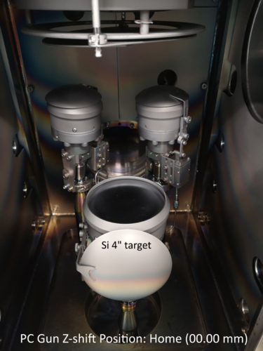 PC Gun Z-shift Position: Home (00.00 mm).
 -
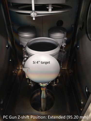 PC Gun Z-shift Position: Extended (95.20 mm).


Characterization (RF mode)
Spectroscopic ellipsometry (RF mode)
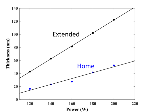
Thicknesses have been measured by spectroscopic ellipsometry (VASE ellipsometer) across different locations on 6" Si wafer with 300nm dry SiO2. The optical model is based on Tauc-Lorentz and two Lorentz oscillators. The deposition parameters are present in the recipe written above. The results are present in a table below:
| PC Gun Z-shift Position: Extended (95.20 mm) | |||||||
|---|---|---|---|---|---|---|---|
| Deposition conditions
Power (W) |
Time (s) | Pressure (mTorr) | Average (nm) | Standard deviation | Minimum Thickness (nm) | Maximum Thickness (nm) | Rate (nm/s) |
| 120 W | 1800 | 3 | 42.73 | 2.22 | 38.26 | 45.24 | 0.024 |
| 140 W | 1800 | 3 | 62.66 | 2.51 | 56.89 | 65.52 | 0.035 |
| 160 W | 1800 | 3 | 81.23 | 3.17 | 74.56 | 84.54 | 0.045 |
| 180 W | 1800 | 3 | 102.03 | 3.13 | 95.17 | 105.27 | 0.057 |
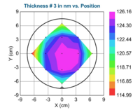
| 200 W | 1800 | 3 | 122.32 | 3.65 | 114.99 | 126.16 | 0.068 |
| PC Gun Z-shift Position: Home (00.00 mm) | |||||||
|---|---|---|---|---|---|---|---|
| Deposition conditions
Power (W) |
Time (s) | Pressure (mTorr) | Average (nm) | Standard deviation | Minimum Thickness (nm) | Maximum Thickness (nm) | Rate (nm/s) |
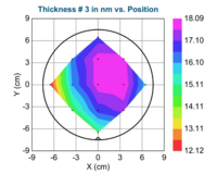
| 120 W | 1800 | 3 | 16.36 | 1.69 | 12.12 | 18.09 | 0.009 |
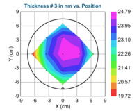
| 140 W | 1800 | 3 | 23.06 | 1.42 | 19.72 | 24.79 | 0.013 |
| 160 W | 1800 | 3 | 27.50 | 1.22 | 24.57 | 28.96 | 0.015 |
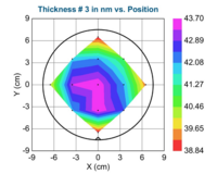
| 180 W | 1800 | 3 | 41.48 | 1.75 | 38.84 | 43.70 | 0.023 |
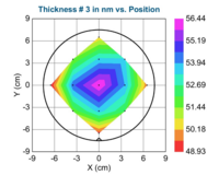
| 200 W | 1800 | 3 | 52.23 | 2.24 | 48.93 | 56.44 | 0.029 |
Deposition rate (RF mode)
- Effect of power on deposition rate (for two different Gun Z-shift Positions).
-
 Measured thickness vs. power.
 -
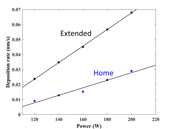 Deposition rate as a function of power.


- PC Gun Z-shift Position: Extended (95.20 mm)
Deposition rate (nm/s) =

- PC Gun Z-shift Position: Home (00.00 mm)
Deposition rate (nm/s) =

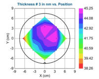
Uniformity (RF mode)
- Uniformity of deposited Si layer across 6-inch wafer.
-
 120 W; PC Gun Z-shift Position: Extended (95.20 mm)
 -
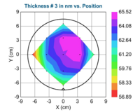 140 W; PC Gun Z-shift Position: Extended (95.20 mm)
 -
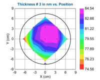 160 W; PC Gun Z-shift Position: Extended (95.20 mm)
 -
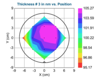 180 W; PC Gun Z-shift Position: Extended (95.20 mm)
 -
 200 W; PC Gun Z-shift Position: Extended (95.20 mm)
 -
 120 W; PC Gun Z-shift Position: Home (00.00 mm)
 -
 140 W; PC Gun Z-shift Position: Home (00.00 mm)
 -
 160 W; PC Gun Z-shift Position: Home (00.00 mm)
 -
 180 W; PC Gun Z-shift Position: Home (00.00 mm)
 -
 200 W; PC Gun Z-shift Position: Home (00.00 mm)


Optical functions (RF mode)
- Optical constants of deposited Si layer.
-
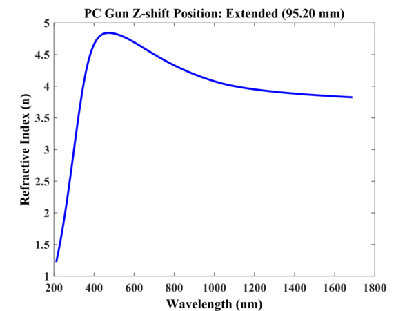 Refractive index (extended position).
 -
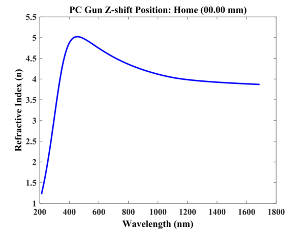 Refractive index (home position).
 -
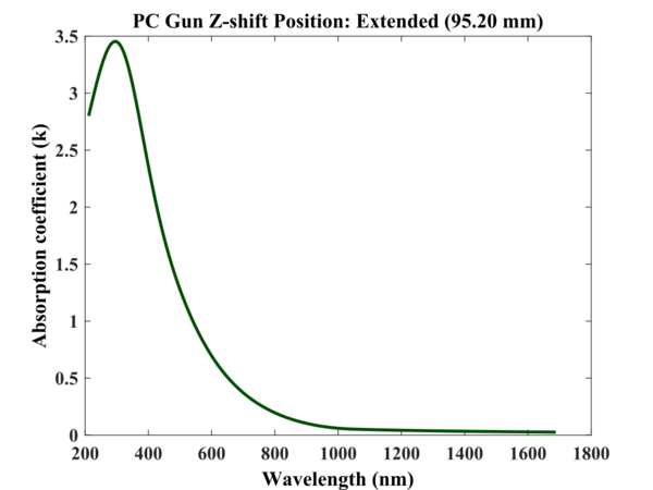 Absorption coefficient (extended position).
 -
 Absorption coefficient (home position).


DC Bias recordings (RF mode)
Any deposition recipe the user runs on Cluster Lesker is getting recorded. Many parameters are stored in the datalog files (in the 1-second interval) that can be accessed and viewed later. Here the DC bias was monitored for the whole experiment.
- DC bias recordings.
-
 DC bias variation during the process for different powers (Extended gun position case).
 -
 DC bias variation during the process for different powers (Home gun position case).


Pulsed DC Sputtering of Si in Sputter-System Metal-Nitride(PC3)
This section covers the results from the pulsed DC deposition method. It must be mentioned that the lower powers give an unstable plasma and varying DC Bias voltage. This is why it is strongly recommended to run this process at the range of 180W-200W (although not higher since the target can only withstand 20 W/cm2 power density which means the maximum power of approximately 200W for a 4-inch target ). Besides, it is also challenging to ignite and maintain plasma using the pulsed-DC power supply at the very beginning of the process, where the power values are still low. It is strongly recommended to ramp the power with the opened source shutter.
The Pulsed-DC Si process recipe in a Sputter-System Metal-Nitride(PC3) is following:
* Recipe Name: MD PC3_Src1 - Pulse DC_Upstream
- PC Gun Z-shift Position: Home (00.00 mm) and Extended (95.20 mm)
- Tilt: No (Target in horizontal plane)
- Deposition mode: Upstream
- Rotation speed: 10 rpm
- Pressure: 3 mTorr
- Power: 120-200 W (It is recomended to use 200W for for the most stable DC bias voltage).
- Frequency: 100 kHz
- Reverse time: 1 µs
- Deposition time: 1800s
- Deposition temperature: room temperature
Samples: 6" Si with 300nm SiO2 (from furnace C1 recipe: DRY1100 05:00:00 + 20 min annealing)
- The photography of Si target mounted in 4” magnetron (PC3 Src1).
-
PC Gun Z-shift Position: Home (00.00 mm).
-
PC Gun Z-shift Position: Extended (95.20 mm).
Characterization (p-DC)
Spectroscopic ellipsometry (p-DC)
Thicknesses have been measured by spectroscopic ellipsometry (VASE ellipsometer) across different locations on 6" Si wafer with 300nm dry SiO2. The optical model is based on Tauc-Lorentz and two Lorentz oscillators. The deposition parameters are present in the recipe written above. The results are present in a table below:
| PC Gun Z-shift Position: Extended (95.20 mm) | |||||||
|---|---|---|---|---|---|---|---|
| Deposition conditions
Power (W) |
Time (s) | Pressure (mTorr) | Average (nm) | Standard deviation | Minimum Thickness (nm) | Maximum Thickness (nm) | Rate (nm/s) |
| 120 W | 1800 | 3 | 98.10 | 2.99 | 91.47 | 101.35 | 0.0545 |
| 160 W | 1800 | 3 | 239.87 | 4.26 | 229.95 | 244.61 | 0.1333 |
| 200 W | 1800 | 3 | 311.43 | 5.38 | 299.99 | 316.45 | 0.1730 |
| PC Gun Z-shift Position: Home (00.00 mm) | |||||||
|---|---|---|---|---|---|---|---|
| Deposition conditions
Power (W) |
Time (s) | Pressure (mTorr) | Average (nm) | Standard deviation | Minimum Thickness (nm) | Maximum Thickness (nm) | Rate (nm/s) |
| 120 W | 1800 | 3 | 37.49 | 1.51 | 34.39 | 39.86 | 0.0208 |
| 160 W | 1800 | 3 | 95.83 | 4.27 | 89.54 | 102.62 | 0.0532 |
| 200 W | 1800 | 3 | 134.73 | 6.97 | 123.37 | 145.90 | 0.0748 |
Deposition rate (p-DC)
- Effect of power on deposition rate (for two different Gun Z-shift Positions).
-
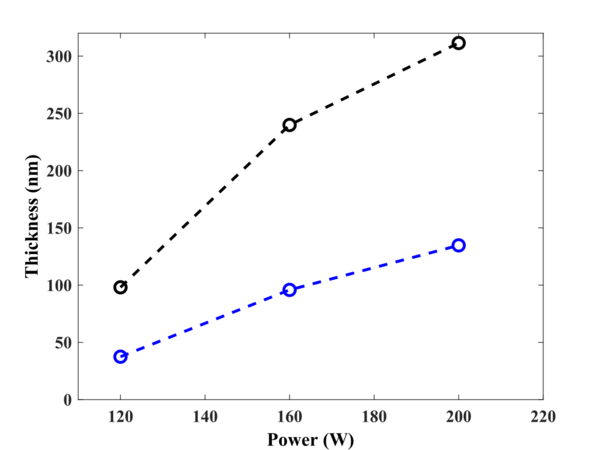 Measured thickness vs. power.
 -
 Deposition rate as a function of power.


Uniformity (p-DC)
- Uniformity of deposited Si layer across 6-inch wafer.
-
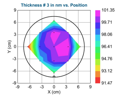 120 W; PC Gun Z-shift Position: Extended (95.20 mm)
 -
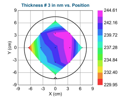 160 W; PC Gun Z-shift Position: Extended (95.20 mm)
 -
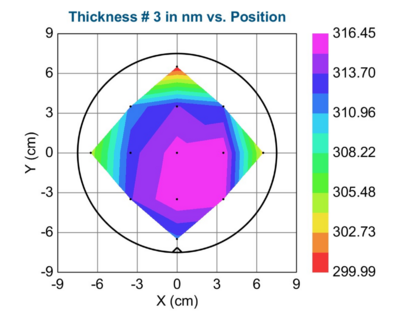 200 W; PC Gun Z-shift Position: Extended (95.20 mm)
 -
 120 W; PC Gun Z-shift Position: Home (00.00 mm)
 -
 160 W; PC Gun Z-shift Position: Home (00.00 mm)
 -
 200 W; PC Gun Z-shift Position: Home (00.00 mm)


Optical functions (p-DC)
- Optical constants of deposited Si layer.
-
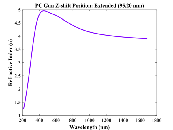 Refractive index (extended position).
 -
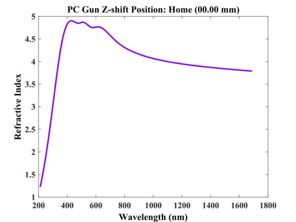 Refractive index (home position).
 -
 Absorption coefficient (extended position).
 -
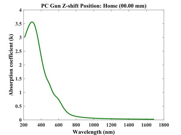 Absorption coefficient (home position).


DC Bias recordings (p-DC)
Any deposition recipe the user runs on Cluster Lesker is getting recorded. Many parameters are stored in the datalog files (in the 1-second interval) that can be accessed and viewed later. Here the DC bias was monitored for the whole experiment.
- DC bias recordings.
-
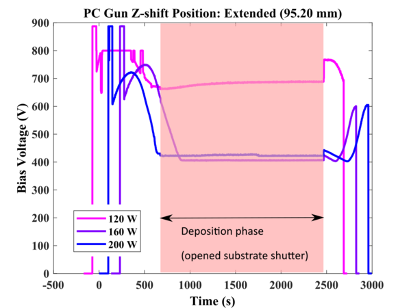 DC bias variation during the process for different powers (Extended gun position case).
 -
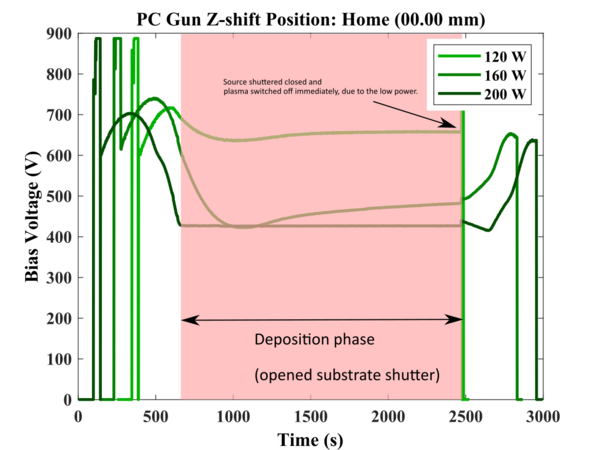 DC bias variation during the process for different powers (Home gun position case).

