Specific Process Knowledge/Etch/III-V ICP/GaAsnano: Difference between revisions
No edit summary |
No edit summary |
||
| (One intermediate revision by one other user not shown) | |||
| Line 1: | Line 1: | ||
'''Feedback to this page''': '''[mailto:labadviser@ | '''Feedback to this page''': '''[mailto:labadviser@nanolab.dtu.dk?Subject=Feed%20back%20from%20page%20http://labadviser.nanolab.dtu.dk/index.php/Specific_Process_Knowledge/Etch/III-V_ICP/GaAsnano click here]''' | ||
<!--Checked for updates on 18/8-2021 - ok/bghe --> | |||
=== GaAs nano etch === | === GaAs nano etch === | ||
Latest revision as of 14:42, 18 August 2021
Feedback to this page: click here
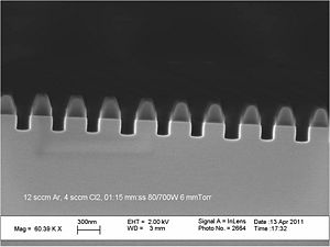
GaAs nano etch
| Recipe | GaAs Nano Etch |
| Cl2 flow | 4 sccm |
| Ar flow | 12 sccm |
| Platen power | 80 W |
| Coil power | 700 W |
| Pressure | 6 mTorr |
| Platen chiller temperature | 20 oC |
| Results (GaAs Nano Etch) from 2011 by Thor Ansbæk @photonic | |
| GaAs | 5 nm/s |
| AlInP | 1 nm/s |
| HSQ | 1.5 nm/s |
| ZEP520a | 2 nm/s |
| Si3N4 | 2 nm/s |
 |
|---|
