Specific Process Knowledge/Etch/DRIE-Pegasus/Pegasus-4/SiO2 Etch: Difference between revisions
| Line 27: | Line 27: | ||
First I need to make sure that the resist work for pattering the aSi layer is good. If the resist is not good the final etch will also not be good. | First I need to make sure that the resist work for pattering the aSi layer is good. If the resist is not good the final etch will also not be good. | ||
==DUV | ==DUV optimization== | ||
Dose test with the doses (J/m2): 200, 210, 220, 230, 240, 250, 270, 280 | Dose test with the doses (J/m2): 200, 210, 220, 230, 240, 250, 270, 280 | ||
The aim was to get good line for 400nm pitch/200nm lines | The aim was to get good line for 400nm pitch/200nm lines | ||
Revision as of 20:58, 23 April 2021
SiO2 Etch using resist as masking material
I am in the process of doing some development of a SiO2 etch. So far I have found this fairly good recipe. For now it is the standard SiO2 etch recipes but I might change the "Standard recipe" a a later time if I find a better one. You are welcome to contact me see more result. I will add them to Labadviser at a later time. /Berit Herstrøm bghe@dtu.dk (Nanolab)
- Recipe name: SiO2_res_10, Recipe no. 10: C06445_02 coil_2500W, platen:300W, He/C4F8= 17.5, C4F8/H2=1, Pressure:8.8mTorr, C4F8:25.6sccm, He:448.7sccm, H2:25.6sccm, 3:56 min
0.4µ/0.2µ
Bad lithography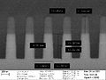
0.5/0.25µ
Etch depth: 652 nm
Resist left: 456 nm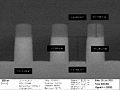
1µ/0.5µ:
Etch depth: 855 nm
Resist left: 487 nm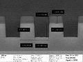
2µ/1µ:
Etch depth: 952 nm
Resist left: 487 nm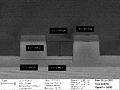
4µ/2µ:
Etch depth: 1106 nm
Resist left: 487 nm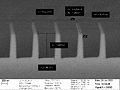
0.8µ/0.2µ
Etch depth: 867 nm
Resist left: 426 nm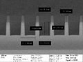
1.0µ/0.25µ:
Etch depth: 893 nm
Resist left: 460 nm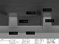
4µ/1µ:
Etch depth: 1033 nm
Resist left: 473 nm


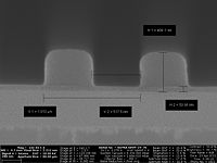
SiO2 Etch using aSi as masking material
I am now starting up development of SiO2 etch using aSi as masking material.
The samples I use are:
- 6" Si afters with oxide (2µm),
- aSi (~300nm),
- Neg. DUV reist (~60nm barc, ~350 nm resist)
- Reticle: Danchip/Triple-D
- Dose 230 J/m2
First I need to make sure that the resist work for pattering the aSi layer is good. If the resist is not good the final etch will also not be good.
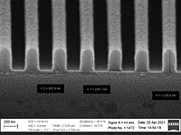
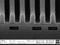
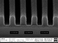
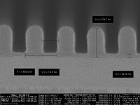
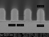
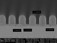
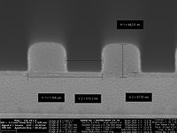
DUV optimization
Dose test with the doses (J/m2): 200, 210, 220, 230, 240, 250, 270, 280 The aim was to get good line for 400nm pitch/200nm lines
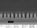
- 400nm pitch 200 nm lines
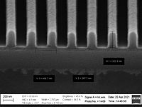
200 J/m2 400nm/268nm
210 J/m2 400nm/239nm
220 J/m2 400nm/208nm
230 J/m2 400nm/209nm
240 J/m2 400nm/215nm
250 J/m2 400nm/207nm
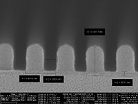
260 J/m2 400nm/188nm
270 J/m2 400nm/155nm
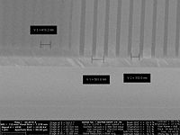
280 J/m2 400nm/0nm


- 1000nm pitch 500 nm lines
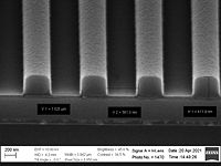
210 J/m2 1000nm/581nm
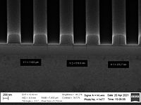
230 J/m2 1000nm/517nm
240 J/m2 1000nm/518nm
250 J/m2 1000nm/510nm
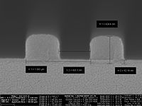
260 J/m2 1000nm/493nm
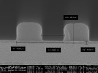
270 J/m2 1000nm/494nm


