Specific Process Knowledge/Thin film deposition/ALD Picosun R200/ZnO deposition using ALD: Difference between revisions
(Created page with "ZnO") |
No edit summary |
||
| Line 1: | Line 1: | ||
ZnO | The ALD window for deposition of zinc oxide (ZnO) ranges from 100 <sup>o</sup>C to 250 <sup>o</sup>C. Several investigation techniques has been implemented for ZnO characterization. Additionally, more information on ZnO can be found on a page about [[Specific_Process_Knowledge/Thin_film_deposition/ALD_Picosun_R200/AZO_deposition_using_ALD|Al-doped ZnO (AZO)]] | ||
All results shown on this page have been obtained using the "ZnOT" recipe on new Si(100) wafers with native oxide: | |||
==Al<sub>2</sub>O<sub>3</sub> standard recipe== | |||
<b>Recipe: AL2O3</b> | |||
<b>Maximum deposition thickness: 100 nm</b> | |||
<b>Temperature: 100 <sup>o</sup>C - 350 <sup>o</sup>C</b> | |||
{| border="2" cellspacing="2" cellpadding="5" align="none" | |||
|- | |||
| | |||
!TMA | |||
!H<sub>2</sub>O | |||
|- | |||
!Nitrogen flow | |||
|150 sccm | |||
|200 sccm | |||
|- | |||
!Pulse time | |||
|0.1 s | |||
|0.1 s | |||
|- | |||
!Purge time | |||
|3.0 s | |||
|4.0 s | |||
|- | |||
|} | |||
This is the standard recipe for deposition of Al<sub>2</sub>O<sub>3</sub> on flat and high aspect ratio structures. For conformal passivation of porous materials, very narrow trenches etc. it is recomanded to use <b>Al2O3T</b> recipe instead. Recipe can be used for deposition in the range 100-350 <sup>o</sup>C. However, at 100 <sup>o</sup>C small amount of carbon impurities has been observed. It is not recomanded to use this recipe for deposition below 100 <sup>o</sup>C, since it also leads to accumulation of H<sub>2</sub>O in the chamber. | |||
===Al<sub>2</sub>O<sub>3</sub> deposition rates=== | |||
The deposition rate for Al<sub>2</sub>O<sub>3</sub> depends on the temperature, see the ALD-window graph below. The uniformity, thickness, refractive index has been obtained using [[Specific_Process_Knowledge/Characterization/Optical_characterization#Ellipsometer|Ellipsometer VASE]]. | |||
<gallery caption="" widths="500px" heights="500px" perrow="2"> | |||
image:ALD_window.jpg| ALD-window for Al<sub>2</sub>O<sub>3</sub> deposition. | |||
image:SE_Al2O3_ALD_typical.JPG| Typical uniformity profile across 100mm Si wafer based on 49 mesurement points. | |||
</gallery> | |||
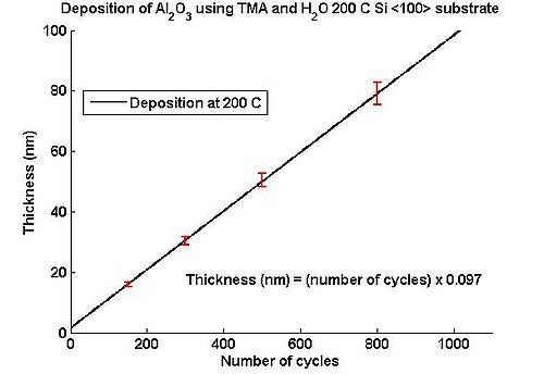
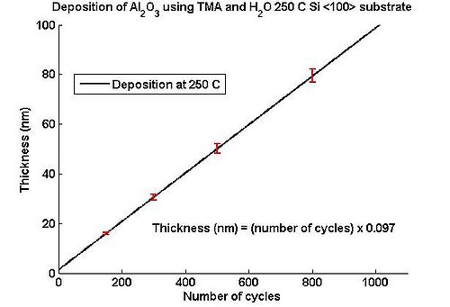
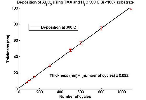
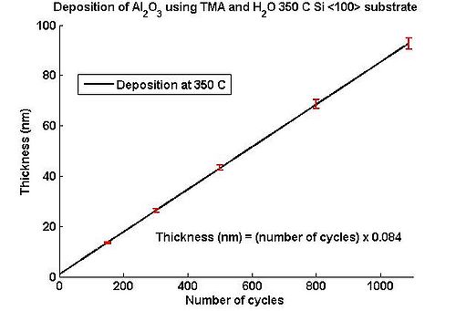
In the graphs below the Al<sub>2</sub>O<sub>3</sub> thickness as function of number of cycles for deposition temperatures between 100 <sup>o</sup>C and 350 <sup>o</sup>C can be seen. From the equations the number of cycles required for a certain thickess can be calculated. | |||
<gallery caption="Aluminium oxide thickness as function of number of cycles" widths="500px" heights="500px" perrow="3"> | |||
image:Al2O3 100C.jpg| Temperature 100 <sup>o</sup>C. | |||
image:Al2O3 150C.jpg| Temperature 150 <sup>o</sup>C. | |||
image:Al2O3 200C.jpg| Temperature 200 <sup>o</sup>C. | |||
</gallery> | |||
<gallery caption="Aluminium oxide thickness as function of number of cycles" widths="500px" heights="500px" perrow="3"> | |||
image:Al2O3 250C.jpg| Temperature 250 <sup>o</sup>C. | |||
image:Al2O3 300C.jpg| Temperature 300 <sup>o</sup>C. | |||
image:Al2O3 350C.jpg| Temperature 350 <sup>o</sup>C. | |||
</gallery> | |||
<br clear="all" /> | |||
<b>Evgeniy Shkondin, DTU Danchip, 2014-2016.</b> | |||
<br clear="all" /> | |||
<br clear="all" /> | |||
===Al<sub>2</sub>O<sub>3</sub> standard recipe characterization across 100 mm Si <100> wafer === | |||
{| border="2" cellspacing="2" cellpadding="3" colspan="10" | |||
|bgcolor="#98FB98" |'''Al<sub>2</sub>O<sub>3</sub> deposition at 100 <sup>o</sup>C and 150 <sup>o</sup>C''' | |||
|- | |||
| | |||
{| {{table}} | |||
| align="center" | | |||
{| border="2" cellspacing="2" cellpadding="3" align="center" style="width:750px" | |||
! colspan="5" |Deposition conditions at 100 <sup>o</sup>C | |||
|- | |||
!Number of cycles | |||
|<b>Thickness (nm)</b> | |||
|<b>Uniformity across 100mm Si substrate (%)</b> | |||
|<b>Standard deviation error</b> | |||
|<b>Refractive index @ 632.8 nm</b> | |||
|- | |||
|150 | |||
|14.11 | |||
|2.18 | |||
|0.225 | |||
|1.56 | |||
|- | |||
|300 | |||
|25.94 | |||
|0.68 | |||
|0.14 | |||
|1.59 | |||
|- | |||
|500 | |||
|41.35 | |||
|1.87 | |||
|0.60 | |||
|1.59 | |||
|- | |||
|800 | |||
|65.05 | |||
|2.28 | |||
|1.13 | |||
|1.59 | |||
|- | |||
|1088 | |||
|87.25 | |||
|2.15 | |||
|1.35 | |||
|1.60 | |||
|- | |||
|} | |||
| align="center" valign="top"| | |||
{| border="2" cellspacing="2" cellpadding="3" align="center" style="width:750px" | |||
! colspan="5" |Deposition conditions at 150 <sup>o</sup>C | |||
|- | |||
!Number of cycles | |||
|<b>Thickness (nm)</b> | |||
|<b>Uniformity across 100mm Si substrate (%)</b> | |||
|<b>Standard deviation error</b> | |||
|<b>Refractive index @ 632.8 nm</b> | |||
|- | |||
|150 | |||
|15.38 | |||
|1.72 | |||
|0.18 | |||
|1.61 | |||
|- | |||
|300 | |||
|28.67 | |||
|1.73 | |||
|0.36 | |||
|1.62 | |||
|- | |||
|500 | |||
|46.93 | |||
|1.75 | |||
|0.57 | |||
|1.62 | |||
|- | |||
|800 | |||
|73.46 | |||
|1.75 | |||
|0.92 | |||
|1.63 | |||
|- | |||
|1088 | |||
|99.50 | |||
|1.74 | |||
|1.20 | |||
|1.63 | |||
|- | |||
|} | |||
|- | |||
|} | |||
|} | |||
%%%%%%%%%%%%%%%%%%%%%%%%%%%%%%%%%%%%%%%%%%%%%%%%%%%%%%%%%%%%%%%%%%%%%%%%%%%%%%%%%%%%%%%%%%%%%%%%%%%%%%%%%%%%%%%%%%%%%%%%%%%%%% | |||
{| border="2" cellspacing="2" cellpadding="3" colspan="10" | |||
|bgcolor="#98FB98" |'''Al<sub>2</sub>O<sub>3</sub> deposition at 200 <sup>o</sup>C and 250 <sup>o</sup>C''' | |||
|- | |||
| | |||
{| {{table}} | |||
| align="center" | | |||
{| border="2" cellspacing="2" cellpadding="3" align="center" style="width:750px" | |||
! colspan="5" |Deposition conditions at 200 <sup>o</sup>C | |||
|- | |||
!Number of cycles | |||
|<b>Thickness (nm)</b> | |||
|<b>Uniformity across 100mm Si substrate (%)</b> | |||
|<b>Standard deviation error</b> | |||
|<b>Refractive index @ 632.8 nm</b> | |||
|- | |||
|150 | |||
|16.46 | |||
|2.92 | |||
|0.33 | |||
|1.62 | |||
|- | |||
|300 | |||
|31.09 | |||
|1.53 | |||
|0.34 | |||
|1.63 | |||
|- | |||
|500 | |||
|51.20 | |||
|1.10 | |||
|0.39 | |||
|1.64 | |||
|- | |||
|800 | |||
|79.66 | |||
|1.59 | |||
|0.88 | |||
|1.64 | |||
|- | |||
|1088 | |||
|107.69 | |||
|1.41 | |||
|1.04 | |||
|1.64 | |||
|- | |||
|} | |||
| align="center" valign="top"| | |||
{| border="2" cellspacing="2" cellpadding="3" align="center" style="width:750px" | |||
! colspan="5" |Deposition conditions at 250 <sup>o</sup>C | |||
|- | |||
!Number of cycles | |||
|<b>Thickness (nm)</b> | |||
|<b>Uniformity across 100mm Si substrate (%)</b> | |||
|<b>Standard deviation error</b> | |||
|<b>Refractive index @ 632.8 nm</b> | |||
|- | |||
|150 | |||
|16.41 | |||
|0.83 | |||
|0.10 | |||
|1.63 | |||
|- | |||
|300 | |||
|30.81 | |||
|1.13 | |||
|0.24 | |||
|1.64 | |||
|- | |||
|500 | |||
|50.48 | |||
|1.10 | |||
|0.40 | |||
|1.64 | |||
|- | |||
|800 | |||
|79.84 | |||
|1.11 | |||
|0.60 | |||
|1.65 | |||
|- | |||
|1088 | |||
|108.03 | |||
|1.11 | |||
|0.61 | |||
|1.65 | |||
|- | |||
|} | |||
|- | |||
|} | |||
|} | |||
%%%%%%%%%%%%%%%%%%%%%%%%%%%%%%%%%%%%%%%%%%%%%%%%%%%%%%%%%%%%%%%%%%%%%%%%%%%%%%%%%%%%%%%%%%%%%%%%%%%%%%%%%%%%%%%%%%%%%%%%%%%%%% | |||
{| border="2" cellspacing="2" cellpadding="3" colspan="10" | |||
|bgcolor="#98FB98" |'''Al<sub>2</sub>O<sub>3</sub> deposition at 300 <sup>o</sup>C and 350 <sup>o</sup>C''' | |||
|- | |||
| | |||
{| {{table}} | |||
| align="center" | | |||
{| border="2" cellspacing="2" cellpadding="3" align="center" style="width:750px" | |||
! colspan="5" |Deposition conditions at 300 <sup>o</sup>C | |||
|- | |||
!Number of cycles | |||
|<b>Thickness (nm)</b> | |||
|<b>Uniformity across 100mm Si substrate (%)</b> | |||
|<b>Standard deviation error</b> | |||
|<b>Refractive index @ 632.8 nm</b> | |||
|- | |||
|150 | |||
|15.59 | |||
|2.11 | |||
|0.24 | |||
|1.63 | |||
|- | |||
|300 | |||
|29.00 | |||
|0.79 | |||
|0.17 | |||
|1.65 | |||
|- | |||
|500 | |||
|47.86 | |||
|1.71 | |||
|0.26 | |||
|1.64 | |||
|- | |||
|800 | |||
|75.04 | |||
|0.90 | |||
|0.55 | |||
|1.65 | |||
|- | |||
|1088 | |||
|101.76 | |||
|0.75 | |||
|0.62 | |||
|1.65 | |||
|- | |||
|} | |||
| align="center" valign="top"| | |||
{| border="2" cellspacing="2" cellpadding="3" align="center" style="width:750px" | |||
! colspan="5" |Deposition conditions at 350 <sup>o</sup>C | |||
|- | |||
!Number of cycles | |||
|<b>Thickness (nm)</b> | |||
|<b>Uniformity across 100mm Si substrate (%)</b> | |||
|<b>Standard deviation error</b> | |||
|<b>Refractive index @ 632.8 nm</b> | |||
|- | |||
|150 | |||
|13.88 | |||
|0.69 | |||
|0.06 | |||
|1.67 | |||
|- | |||
|300 | |||
|26.70 | |||
|0.62 | |||
|0.12 | |||
|1.64 | |||
|- | |||
|500 | |||
|43.70 | |||
|0.42 | |||
|0.15 | |||
|1.64 | |||
|- | |||
|800 | |||
|68.77 | |||
|0.65 | |||
|0.37 | |||
|1.65 | |||
|- | |||
|1088 | |||
|92.88 | |||
|0.70 | |||
|0.48 | |||
|1.66 | |||
|- | |||
|} | |||
|- | |||
|} | |||
|} | |||
<br clear="all" /> | |||
<b>Evgeniy Shkondin, DTU Danchip, 2014-2016.</b> | |||
<br clear="all" /> | |||
<br clear="all" /> | |||
===Al<sub>2</sub>O<sub>3</sub> XPS investigation for elemental trace analysis=== | |||
XPS profile for Al<sub>2</sub>O<sub>3</sub> has been obtained using [[Specific_Process_Knowledge/Characterization/XPS#XPS-ThermoScientific|XPS-ThermoScientific]]. Al<sub>2</sub>O<sub>3</sub> samples reveals chemically high quality films with no observable contaminations in temperature range 150 - 350 <sup>o</sup>C. At lower temperature (100 <sup>o</sup>C) the ALD reaction starts to become unsufficient and some amount of carbon from TMA precursor gets absorbed into the film. | |||
<gallery caption="" widths="500px" heights="500px" perrow="3"> | |||
image:Al2O3_XPS.jpg| Survey scan of Al<sub>2</sub>O<sub>3</sub>. | |||
image:LT_Al2O3_Carbon_content.JPG| <b>C 1s</b> scan of Al<sub>2</sub>O<sub>3</sub> film deposited at 100<sup>o</sup>C. Shows clearly carbon impurities in the film | |||
image:HT_Al2O3_Carbon_content.JPG| <b>C 1s</b> scan of Al<sub>2</sub>O<sub>3</sub> film deposited between 150<sup>o</sup>C - 350<sup>o</sup>C. No carbon observes. | |||
</gallery> | |||
<br clear="all" /> | |||
<b>Evgeniy Shkondin, DTU Danchip, 2014-2016.</b> | |||
<br clear="all" /> | |||
<br clear="all" /> | |||
Revision as of 19:38, 16 March 2017
The ALD window for deposition of zinc oxide (ZnO) ranges from 100 oC to 250 oC. Several investigation techniques has been implemented for ZnO characterization. Additionally, more information on ZnO can be found on a page about Al-doped ZnO (AZO)
All results shown on this page have been obtained using the "ZnOT" recipe on new Si(100) wafers with native oxide:
Al2O3 standard recipe
Recipe: AL2O3
Maximum deposition thickness: 100 nm
Temperature: 100 oC - 350 oC
| TMA | H2O | |
|---|---|---|
| Nitrogen flow | 150 sccm | 200 sccm |
| Pulse time | 0.1 s | 0.1 s |
| Purge time | 3.0 s | 4.0 s |
This is the standard recipe for deposition of Al2O3 on flat and high aspect ratio structures. For conformal passivation of porous materials, very narrow trenches etc. it is recomanded to use Al2O3T recipe instead. Recipe can be used for deposition in the range 100-350 oC. However, at 100 oC small amount of carbon impurities has been observed. It is not recomanded to use this recipe for deposition below 100 oC, since it also leads to accumulation of H2O in the chamber.
Al2O3 deposition rates
The deposition rate for Al2O3 depends on the temperature, see the ALD-window graph below. The uniformity, thickness, refractive index has been obtained using Ellipsometer VASE.
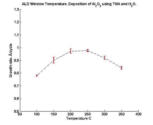
ALD-window for Al2O3 deposition.
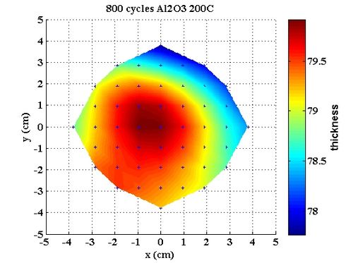
Typical uniformity profile across 100mm Si wafer based on 49 mesurement points.


In the graphs below the Al2O3 thickness as function of number of cycles for deposition temperatures between 100 oC and 350 oC can be seen. From the equations the number of cycles required for a certain thickess can be calculated.
- Aluminium oxide thickness as function of number of cycles
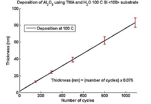
Temperature 100 oC.
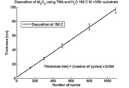
Temperature 150 oC.
Temperature 200 oC.


- Aluminium oxide thickness as function of number of cycles
Temperature 250 oC.
Temperature 300 oC.
Temperature 350 oC.


Evgeniy Shkondin, DTU Danchip, 2014-2016.
Al2O3 standard recipe characterization across 100 mm Si <100> wafer
| Al2O3 deposition at 100 oC and 150 oC | ||||||||||||||||||||||||||||||||||||||||||||||||||||||||||||||||||||||||
|
| ||||||||||||||||||||||||||||||||||||||||||||||||||||||||||||||||||||||||
%%%%%%%%%%%%%%%%%%%%%%%%%%%%%%%%%%%%%%%%%%%%%%%%%%%%%%%%%%%%%%%%%%%%%%%%%%%%%%%%%%%%%%%%%%%%%%%%%%%%%%%%%%%%%%%%%%%%%%%%%%%%%%
| Al2O3 deposition at 200 oC and 250 oC | ||||||||||||||||||||||||||||||||||||||||||||||||||||||||||||||||||||||||
|
| ||||||||||||||||||||||||||||||||||||||||||||||||||||||||||||||||||||||||
%%%%%%%%%%%%%%%%%%%%%%%%%%%%%%%%%%%%%%%%%%%%%%%%%%%%%%%%%%%%%%%%%%%%%%%%%%%%%%%%%%%%%%%%%%%%%%%%%%%%%%%%%%%%%%%%%%%%%%%%%%%%%%
| Al2O3 deposition at 300 oC and 350 oC | ||||||||||||||||||||||||||||||||||||||||||||||||||||||||||||||||||||||||
|
| ||||||||||||||||||||||||||||||||||||||||||||||||||||||||||||||||||||||||
Evgeniy Shkondin, DTU Danchip, 2014-2016.
Al2O3 XPS investigation for elemental trace analysis
XPS profile for Al2O3 has been obtained using XPS-ThermoScientific. Al2O3 samples reveals chemically high quality films with no observable contaminations in temperature range 150 - 350 oC. At lower temperature (100 oC) the ALD reaction starts to become unsufficient and some amount of carbon from TMA precursor gets absorbed into the film.
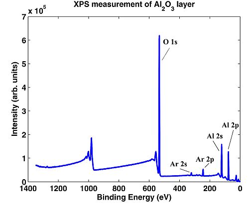
Survey scan of Al2O3.
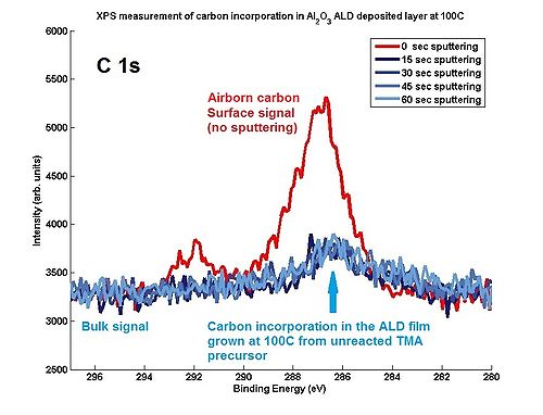
C 1s scan of Al2O3 film deposited at 100oC. Shows clearly carbon impurities in the film
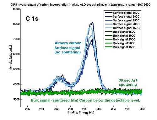
C 1s scan of Al2O3 film deposited between 150oC - 350oC. No carbon observes.


Evgeniy Shkondin, DTU Danchip, 2014-2016.