Specific Process Knowledge/Lithography/CSAR: Difference between revisions
| Line 222: | Line 222: | ||
|- | |- | ||
|-style="background:red; color:White" | |-style="background:red; color:White" | ||
!colspan="7"|AllResist CSAR 1:1 in anisole (< 2ml per 4" wafer), Spin Coater: Manual LabSpin A-5, TIGRE, 16-06-2014. Softbake 2 min @ 150 degC. | !colspan="7"|AllResist CSAR 6200.09 1:1 in anisole (< 2ml per 4" wafer), Spin Coater: Manual LabSpin A-5, TIGRE, 16-06-2014. Softbake 2 min @ 150 degC. | ||
|- | |- | ||
| Line 276: | Line 276: | ||
|- | |- | ||
|-style="background:green; color:White" | |-style="background:green; color:White" | ||
!colspan="7"|AllResist CSAR | !colspan="7"|AllResist CSAR 6200.18 (< 2ml per 4" wafer), Spin Coater: Manual Standard Resists, E-5, TIGRE, 15-06-2016. Softbake 2 min @ 180 degC. | ||
|- | |- | ||
Revision as of 15:30, 4 July 2016
| Resist | Polarity | Manufacturer | Comments | Technical reports | Spinner | Developer | Rinse | Remover | Process flows (in docx-format) |
| CSAR | Positive | AllResist | Standard positive resist, very similar to ZEP520. | Allresist_CSAR62_English.pdf,, CSAR_62_Abstract_Allresist.pdf | Manual Spinner 1 (Laurell), Spin Coater Labspin | XAR-600-546, XAR-600-548, N50, MIBK:IPA | IPA | AR-600-71, 1165 Remover | Process Flow CSAR.docx |
Simple e-beam pattern in this resist has been tested, the results showed on this page. If you have questions to the process or wish to use this e-beam resist, please contact Tine Greibe at tigre@danchip.dtu.dk.
Process Flow
| Equipment | Process Parameters | Comments | |
|---|---|---|---|
| Pretreatment | |||
| 4" Si wafers | No Pretreatment | ||
| Spin Coat | |||
| Spin Coater Manual, LabSpin, A-5 | AR-P 6200/2 AllResist E-beam resist
60 sec at various spin speed. Acceleration 4000 s-2, softbake 1 - 5 min at 150 deg Celcius |
Disposal pipette used; clean by N2-gun before use. Use approximately 1.5 ml per 4" wafer, never use a pipette twice. Softbake is not a crucial step, see e-mail correspondence with AllResist here. | |
| Characterization | |||
| Ellipsometer VASE B-1 | 9 points measured on 100 mm wafer | ZEP program used; measured at 70 deg only | |
| E-beam Exposure | |||
| JEOL 9500 E-beam writer, E-1 | Dosepattern 15nm - 100nm,
dose 120-350 muC/cm2 |
Virtual chip mark height detection (CHIPAL V1) used in corner of every dose array | |
| Development | |||
| Fumehood, D-3 | 60 sec in X AR 600-546,
60 sec rinse in IPA, N2 Blow dry |
Gentle agitation while developing. After developing, wafer is immersed in beaker with IPA, subsequently blow dried with N2 gun. | |
| Characterization | |||
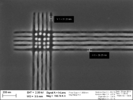
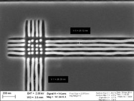
| Zeiss SEM Supra 60VP, D-3 | 2-3 kV, shortest working distance possible, chip mounted with Al tape | For dosepattern SEM inspection: the wafers are diced into smaller pieces and sputter coated with Pt at DTU CEN before SEM inspection; please contact Ramona Valentina Mateiu for further information. | |
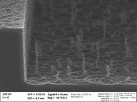
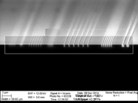
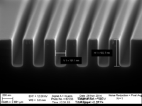
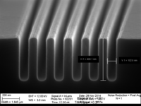
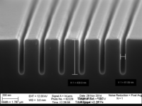
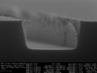
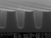
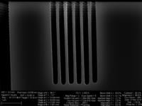
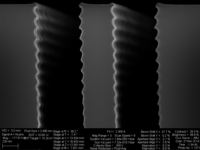
| Residues: After a dry etch, residues are very easily observed by SEM inspection. This particular trench was e-beam patterned at a too low dose. Residues are recommended removed by optimising dose and developing, not by plasma ashing, since our plasma ashers in the cleanroom are 'dirty' and most likely generate particles on the substrate. |
Spin Curves
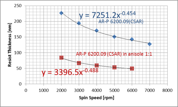
The thickness is measured on VASE Ellipsometer using a simple Cauchy model for a transparent polymer on Si. The measurements are performed at one incidence angle (70 degrees) only. 9 points on each 4" wafer has been measured; the standard deviation thus representing the homogeinity of the film on the 4" wafers.
Please be aware that I have experienced a somewhat large thickness deviation (5-8 %) depending on the amount of resist applied to the wafer before spin coating.
| AllResist AR-P 6200.09 (> 2ml per 4" wafer) spinning on Spin Coater: Manual LabSpin A-5, TIGRE, 09-04-2014. Softbake 5 min @ 150 degC. | ||||||
|---|---|---|---|---|---|---|
| Spin Speed [rpm] | Acceleration [1/s2] | Thickness [nm] | ||||
| 2000 | 4000 | 226 | ||||
| 3000 | 4000 | 194 | ||||
| 4000 | 4000 | 170 | ||||
| 5000 | 4000 | 151 | ||||
| 6000 | 4000 | 142 | ||||
| 7000 | 4000 | 127 | ||||
| AllResist CSAR 6200.09 1:1 in anisole (< 2ml per 4" wafer), Spin Coater: Manual LabSpin A-5, TIGRE, 16-06-2014. Softbake 2 min @ 150 degC. | ||||||
|---|---|---|---|---|---|---|
| Spin Speed [rpm] | Acceleration [1/s2] | Thickness [nm] | ||||
| 2000 | 4000 | 84 | ||||
| 3000 | 4000 | 67 | ||||
| 4000 | 4000 | 59 | ||||
| 5000 | 4000 | 53 | ||||
| 6000 | 4000 | 49 | ||||
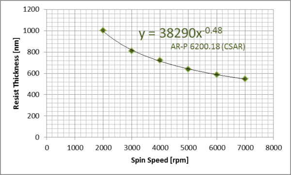
| AllResist CSAR 6200.18 (< 2ml per 4" wafer), Spin Coater: Manual Standard Resists, E-5, TIGRE, 15-06-2016. Softbake 2 min @ 180 degC. | ||||||
|---|---|---|---|---|---|---|
| Spin Speed [rpm] | Acceleration [1/s2] | Thickness [nm] | ||||
| 2000 | 2000 | 1003 | ||||
| 3000 | 2000 | 809 | ||||
| 4000 | 2000 | 721 | ||||
| 5000 | 2000 | 639 | ||||
| 6000 | 2000 | 586 | ||||
| 7000 | 2000 | 549 | ||||
Contrast Curves
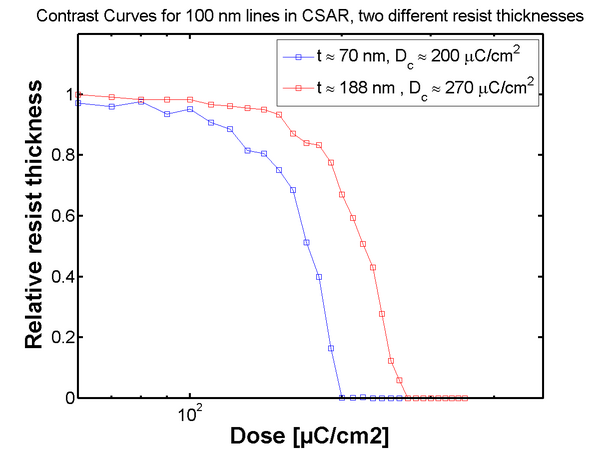
100 nm lines in both ~70 nm and ~188 nm thick CSAR has been developed with AR-600-546 (standard CSAR developer) at room temperature.
| CSAR Contrast Curve, Processed by TIGRE, FEB-MARCH 2016 | ||||
|---|---|---|---|---|
| Resist | Spin Coat | E-beam exposure | Development | Characterisation |
| CSAR AR-P6200 AllResist, CSAR AR-P6200 diluted 1:1 in Anisole | 08-02-2016, LabSpin E-5, 4000 rpm, 60s, softbaked 60s @ 205 degC | 09-02-2016, JBX9500 E-2, 2nA aperture 5, doses 40-600 µC/cm2, 100 nm lines and 300 nm spaces | 11-02-2016, Fumehood D-2, AR-600-546, rinsed in IPA 60s. | 02-03-2016 AFM Icon, F-2, ScanAsyst in Air |
Dark Erosion
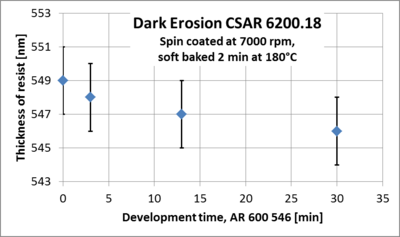
Dark erosion has been measured on a un-exposed 4" wafer spin coated with CSAR 6200.18 to a thickness of approximately 549 nm. The resist thickness has been measured by VASE Ellipsometer before development, and after 3 minutes, 13 minutes, and 30 minutes of development in AR 600 546.
The graphs shows the measured thicknesses; the errorbars represents the standard deviations from the ellipsometric measurements. The average etch rate of CSAR is ~0.1 nm/min.
Dosetests
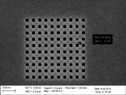
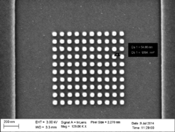
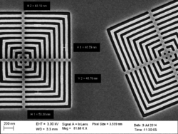
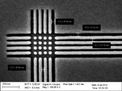
So far (September 2014) three wafers with CSAR have been e-beam exposed with dosetests and inspected in SEM. Thickness of resist, e-beam dose and development time has been changed somewhat from wafer to wafer:
style = "border-radius: 6px; border: 3px solid #000000;
| Process | Equipment | Parameters | ||
|---|---|---|---|---|
| 6.13 | 4.09 | 3.05 | ||
| Resist | Fumehood D-3 | Resist: AR-P 6200/2 diluted 1:1 in anisole (Bottled opened 16-06-2014 TIGRE) | Resist: AR-P 6200/2 diluted 1:1 in anisole (Bottled opened 16-06-2014 TIGRE) | Resist: AR-P 6200/2 |
| Spin Coat | Spin Coater LabSpin A-5 | Spin: 1 min @ 6000 rpm, softbake: 1 min @ 150 degC, thickness: ~50nm (27-08-2014 TIGRE) |
Spin: 1 min @ 5000 rpm, softbake: 2 min @ 150 degC, thickness: ~53nm (16-06-2014 TIGRE) |
Spin: 1 min @ 6000 rpm, softbake: 5 min @ 150 degC, thickness: ~143nm (09-04-2014 TIGRE) |
| E-beam exposure | JEOL 9500 E-2 | Condition file: 0.2nA_ap5, doses: 180-420 muC/cm2, Shot pitch: 7-27 nm, PEC: no (27-08-2014 TIGRE) |
Condition file: 0.2nA_ap5, doses: 207-242 muC/cm2, Shot pitch: 5 nm, PEC: no (02-07-2014 TIGRE) |
Condition file: 2nA_ap5, doses: 207-242 muC/cm2, Shot pitch: 5 nm, PEC: no (10-04-2014 TIGRE) |
| Develop | Fumehood D-3 | Developer: SX-AR 600-54/6, time: 30 sec, Rinse: 30 sec in IPA (28-08-2014 TIGRE) |
Developer: SX-AR 600-54/6, time: 60 sec, Rinse: 30 sec in IPA (08-07-2014 TIGRE) |
Developer: SX-AR 600-54/6, time: 60 sec, Rinse: 60 sec in IPA (April/May-2014 TIGRE) |
| Sputter Coat (please contact Ramona Valentina Mateiu for information ) | Cressington 208HR, DTU CEN | 3-5 nm Pt, sputtering, (29-08-2014 TIGRE) | 3-5 nm Pt, sputtering (09-07-2014 TIGRE) | 3-5 nm Pt, sputtering (22-05-2014 TIGRE) |
| Characterization | Zeiss SEM Supra 60VP, D-3 | Acc voltage: 3 kV, WD: < 4mm, conducting tape close to pattern (29-08-2014 TIGRE) |
Acc voltage: 3 kV, WD: < 4mm, conducting tape close to pattern (09-07-2014 TIGRE) |
Acc voltage: 2 kV, WD: < 4mm, conducting tape close to pattern (06-06-2014 TIGRE) |
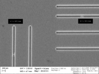
SEM inspection
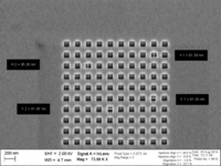
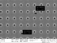
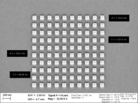
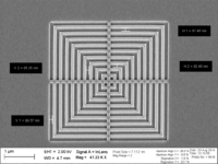
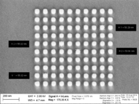
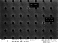
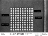
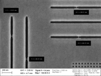
| SEM inspection of wafer 6.13, 100 nm exposed pattern, shot pitch 7 nm | |||||||
|---|---|---|---|---|---|---|---|
| 300 [muC/cm2] | 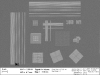
|
|
|
|
|
|
ACHK NOT READY |
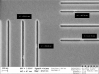
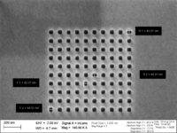
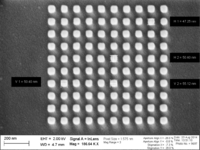
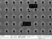
| SEM inspection of wafer 6.13, 50 nm exposed pattern, shot pitch 7 nm | |||||||
|---|---|---|---|---|---|---|---|
| 270 [muC/cm2] | 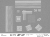
|
|
|
|
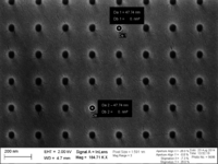
|
ACHK NOT READY | |
| 300 [muC/cm2] | 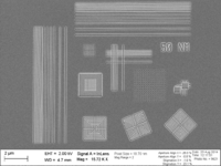
|
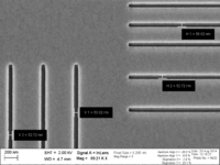
|
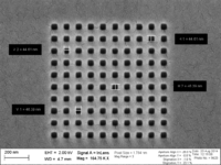
|
|
|
ACHK NOT READY | |
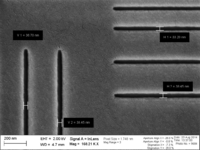
| SEM inspection of wafer 6.13, 30 nm exposed pattern, shot pitch 7 nm | |||||||
|---|---|---|---|---|---|---|---|
| 270 [muC/cm2] | 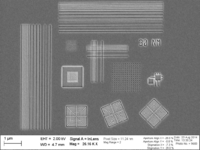
|
|
|
|
ACHK NOT READY | ||
| 300 [muC/cm2] | 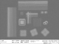
|
|
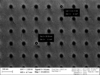
|
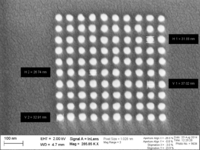
|
ACHK NOT READY | ||
| SEM inspection of wafer 6.13, 20 nm exposed pattern, shot pitch 7 nm | ||||
|---|---|---|---|---|
| 270 [muC/cm2] | 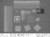
|
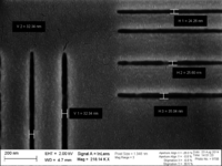
|
ACHK NOT READY | |
| 300 [muC/cm2] | 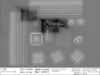
|
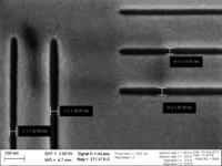
|
ACHK NOT READY | |
| SEM inspection of wafer 4.09, 50 nm exposed pattern, shot pitch 5 nm | ||||||
|---|---|---|---|---|---|---|
| 230 [muC/cm2] | 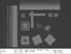
|
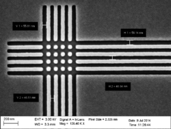
|
|
|
| |
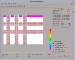
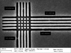
| SEM inspection of wafer 4.09, 30 nm exposed pattern, shot pitch 5 nm | ||||
|---|---|---|---|---|
| 219 [muC/cm2] | 
|
|
| |
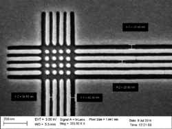
| 230 [muC/cm2] | 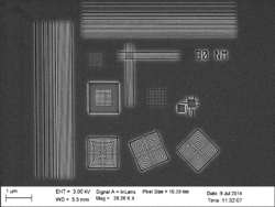
|
|
||
| 242 [muC/cm2] | 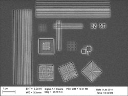
|
|
||
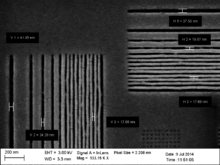
| SEM inspection of wafer 4.09, 20 nm exposed pattern, shot pitch 5 nm | ||||
|---|---|---|---|---|
| 242 [muC/cm2] | 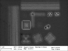
|
|
||
| 253 [muC/cm2] | 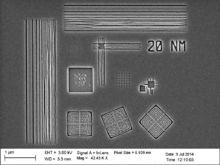
|
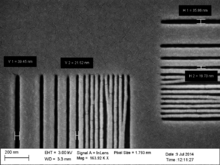
|
||
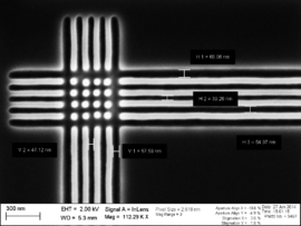
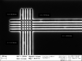
| SEM inspection of wafer 3.05, 50 nm exposed pattern, shot pitch 5 nm | ||||
|---|---|---|---|---|
| 219 [muC/cm2] | 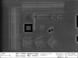
|
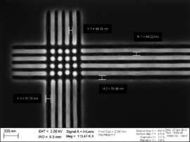
|
||
| 230 [muC/cm2] | 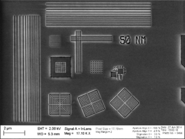
|
|
||
| 242 [muC/cm2] | 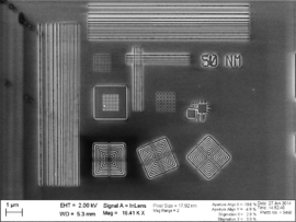
|
|
||
| SEM inspection of wafer 3.05, 30 nm exposed pattern, shot pitch 5 nm | ||||
|---|---|---|---|---|
| 219 [muC/cm2] | 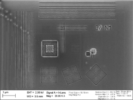
|
|
||
| 230 [muC/cm2] | 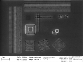
|
|
||
| 242 [muC/cm2] | 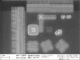
|
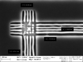
|
||
| SEM inspection of wafer 3.05, 20 nm exposed pattern, shot pitch 5 nm | ||||
|---|---|---|---|---|
| 230 [muC/cm2] | 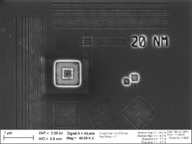
|
|||
| 242 [muC/cm2] | 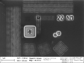
|
|||
| 253 [muC/cm2] | 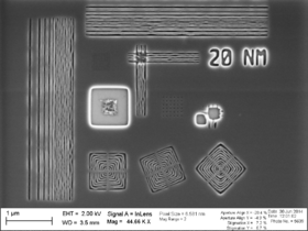
|
|||
Etch Tests
If you have wafers or chips with CSAR you would like to have tested, please send me an [email].
Chlorine versus flourine-based etches
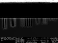
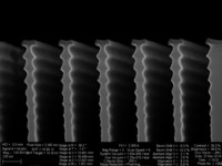
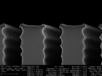
We have experienced problems with removal of CSAR after chlorine-based dry etch, see the file File:DryEtchTestsCSAR.pdf. It seems the chlorine etch forms particles of chlorinated CSAR on the surface, and these particles remains on the surface after resist removal with AR-600-71. The C4F8/SF6 etch also forms particles on the surface, but much smaller than those formed in the chlorine etch. It seems these particles are removed after 3 minutes in AR-600-71.
How to mount chips in dry etch tools
All etch rates presented here are measured on chips (i.e. diced 4" wafers) crystal bonded to a carrier. The carrier is either a blank Si wafer, a Si wafer spin coated with resist or a Si wafer coated with ALD grown Al2O3.
| Sample | CSAR Etch rate nm/min |
|---|---|
| Full 4" Si wafer with non-patterned ~180 nm CSAR | ~56.5 (based on 2 runs) |
| Full 4" Si wafer with non-patterned ~240 nm CSAR, postbaked 60 sec @ 130 degC |
~56.5 (based on 2 runs) |
| 1/4 4" Si wafer with non-patterned ~125 nm CSAR, not crystal bonded to Si carrier |
~83.3 (based on 3 runs) |
| 1/4 4" Si wafer with non-patterned ~125 CSAR, crystal bonded to 4" Si carrier |
~54 (based on 1 run) |
Etch rates and profile inspection
Continous Etches
