Specific Process Knowledge/Etch/Etching of Silicon Oxide/SiO2 etch using AOE/Standard recipe with resist mask/Striation: Difference between revisions
< Specific Process Knowledge | Etch | Etching of Silicon Oxide | SiO2 etch using AOE | Standard recipe with resist mask
Jump to navigation
Jump to search
| Line 12: | Line 12: | ||
#* Resist edge gets rough during etching due to plasma heating (out-gassing while the surface get UV hardened. This make the resist crumple). | #* Resist edge gets rough during etching due to plasma heating (out-gassing while the surface get UV hardened. This make the resist crumple). | ||
#*The edge can maybe also get roughened due to sputtering. | #*The edge can maybe also get roughened due to sputtering. | ||
<br clear="all"/> | |||
==Sidewall roughness and resist surface after etch viewed with SEM== | ==Sidewall roughness and resist surface after etch viewed with SEM== | ||
Revision as of 09:02, 20 April 2016
Feedback to this page: click here
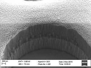
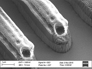
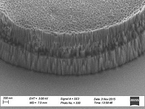
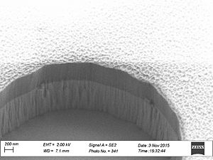
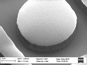
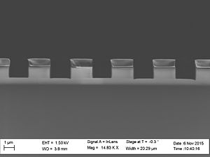
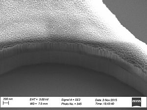
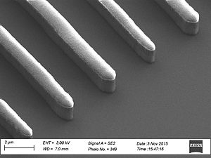
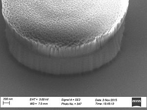
Striation: Side wall roughness
When etching silicon oxide rough sidewalls are most often seem. This effect is called striation, because it creates stripes along the etched profile. The literature gives several coarses for this. The two main courses seems to be:
- deposition on the sidewalls as the etch proceeds, coursing masking effects
- This can come from flour-carbon polymers from the plasma (some this this layer protects from striation)
- Re-deposition of sputtered SiO2
- damage of the resist mask coursed by plasma heating and/or interaction with the resist. This pattern change at the edge gets transferred to the oxide profile during the etch.
- Resist edge gets rough during etching due to plasma heating (out-gassing while the surface get UV hardened. This make the resist crumple).
- The edge can maybe also get roughened due to sputtering.
Sidewall roughness and resist surface after etch viewed with SEM
- Striation with different resists used
Az resist
Az resist
Az resist
Az resist - profile after etch
Mir resist

Mir resist
Mir resist
Mir resist - profile after etch
nLof
nLof
nLof
nLof resist - profile after etch


Roughness of the resist after etch measured with the AFM
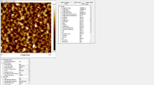
AZ5214E:Ra=3.98nm, Rmax=33,0nm
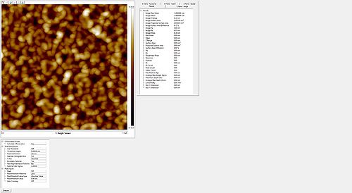
AZ MIR: Ra=4.55nm, Rmax=36.3nm
AZ nLof 2020: Ra=3.31nm, Rmax=28.0nm


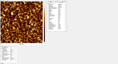
Sidewall roughness/resist surface roughness effected by UV curing and heat treatment of nLof resist 

| AOE etch with nLof resist with different treatments | |||||
| 1 | 2 | 3 | 4 | 5 | |
|---|---|---|---|---|---|
| Treatment | No treatment before AOE etch | No treatment after 5min AOE etch | Flood-E 70s + 1min@110dg | 5min@150dg | Flood-E 70s + 60s@110dg + 5min@150dg |
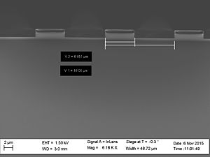
| SEM image | 
|

|

|

|

|
| AFM roughness scan | Ra=2.1nm Rmax=25.1nm 
|
Ra=3.31nm Rmax=28.0nm 
|
Ra=3.34nm Rmax=26.8nm 
|
Ra=2.45nm, Rmax=19.4nm 
|
Ra=2.52nm, Rmax=23.7nm 
|
| D | D1 | D2 | D3 | D4 | D5 |
Sidewall roughness/resist surface roughness effected by UV curing and heat treatment of AZ5214E resist
| AOE etch with AZ5214E resist with different treatments | |||||
| 1 | 2 | 3 | 4 | ||
|---|---|---|---|---|---|
| Treatment | No treatment before AOE etch | No treatment after 5min AOE etch | Flood-E 55s + 120s@110dg | Flood-E 55s + 120s@110dg + 5min@150dg | |
| SEM image | 
|

|

|

| |
| AFM roughness scan | Pre etch: cannot measure | Ra=4.40nm, Rmax=36.5nm 
|
Ra=3.68nm, Rmax=25.6nm 
|
Ra=3.57nm, Rmax=28.5nm 
| |
| D | D1 | D2 | D3 | D4 | |