Specific Process Knowledge/Etch/Etching of Silicon Oxide/SiO2 etch using AOE/Standard recipe with resist mask/Striation: Difference between revisions
< Specific Process Knowledge | Etch | Etching of Silicon Oxide | SiO2 etch using AOE | Standard recipe with resist mask
Jump to navigation
Jump to search
| Line 67: | Line 67: | ||
|- | |- | ||
!AFM roughness scan | !AFM roughness scan | ||
| | |Ra=2.1nm Rmax=25.1nm [[File:nLof0 pre AOE_1_5my.jpg|400px]] | ||
| | |Ra=3.31nm Rmax=28.0nm [[File:nLof1_1.jpg|400px]] | ||
| | |Ra=3.34nm Rmax=26.8nm [[File:nLof2 pretreat1_2.jpg|400px]] | ||
| | |Ra=2.45nm, Rmax=19.4nm [[File:nLof3.jpg|400px]] | ||
| | |Ra=2.52nm, Rmax=23.7nm [[File:nLof4.jpg|400px]] | ||
|- | |- | ||
!D | !D | ||
Revision as of 10:24, 18 April 2016
Feedback to this page: click here
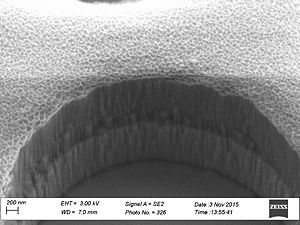
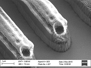
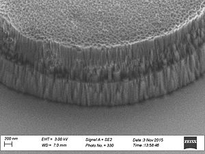
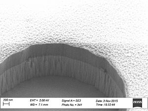
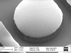
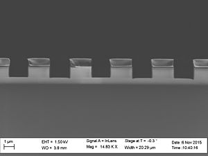
Striation: Side wall roughness
- Striation with different resists used
Az resist
Az resist
Az resist
Az resist - profile after etch
Mir resist

Mir resist
Mir resist
Mir resist - profile after etch
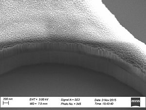
nLof
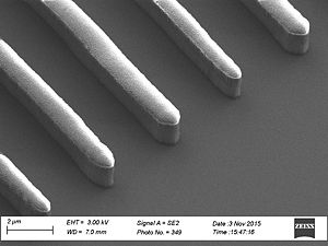
nLof
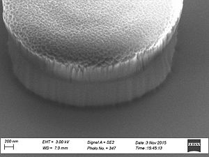
nLof
nLof resist - profile after etch


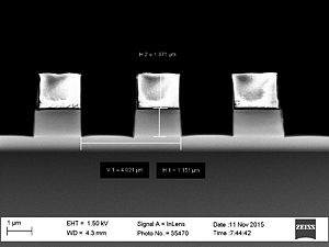
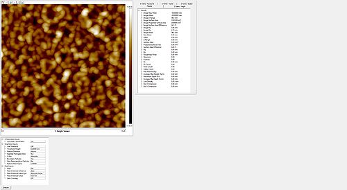
Roughness of the resist after etch measured with the AFM
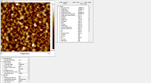
AZ5214E:Ra=3.98nm, Rmax=33,0nm
AZ MIR: Ra=4.55nm, Rmax=36.3nm
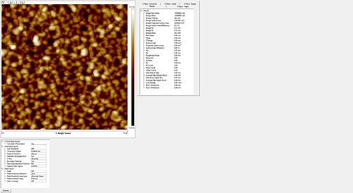
AZ nLof 2020: Ra=3.31nm, Rmax=28.0nm


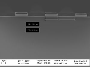
Sidewall roughness effected by UV curing and heat treatment of nLof resist 

| AOE etch with nLof resist with different treatments | |||||
| 1 | 2 | 3 | 4 | 5 | |
|---|---|---|---|---|---|
| Treatment | No treatment before AOE etch | No treatment after 5min AOE etch | Flood-E 70s + 1min@110dg | 5min@150dg | Flood-E 70s + 60s@110dg + 5min@150dg |
| SEM image | 
|

|

|

|

|
| AFM roughness scan | Ra=2.1nm Rmax=25.1nm 
|
Ra=3.31nm Rmax=28.0nm 
|
Ra=3.34nm Rmax=26.8nm 
|
Ra=2.45nm, Rmax=19.4nm 
|
Ra=2.52nm, Rmax=23.7nm 
|
| D | D1 | D2 | D3 | D4 | D5 |