Specific Process Knowledge/Thin film deposition/Deposition of Nickel/Electroplating of nickel: Difference between revisions
| Line 26: | Line 26: | ||
|-style="background:silver; color:black" | |-style="background:silver; color:black" | ||
! | ! | ||
![[Specific_Process_Knowledge/Thin_film_deposition/Deposition_of_Nickel/Electroplating_of_nickel|DCHimm18-03]] | ![[Specific_Process_Knowledge/Thin_film_deposition/Deposition_of_Nickel/Electroplating_of_nickel|DCHimm18.1-03]] | ||
![[Specific_Process_Knowledge/Thin_film_deposition/Deposition_of_Nickel/Electroplating_of_nickel|DCHimm18-04]] | ![[Specific_Process_Knowledge/Thin_film_deposition/Deposition_of_Nickel/Electroplating_of_nickel|DCHimm18.1-04]] | ||
![[Specific_Process_Knowledge/Thin_film_deposition/Deposition_of_Nickel/Electroplating_of_nickel|DCHimm18-06]] | ![[Specific_Process_Knowledge/Thin_film_deposition/Deposition_of_Nickel/Electroplating_of_nickel|DCHimm18.1-06]] | ||
![[Specific_Process_Knowledge/Thin_film_deposition/Deposition_of_Nickel/Electroplating_of_nickel|DCHimm18-12]] | ![[Specific_Process_Knowledge/Thin_film_deposition/Deposition_of_Nickel/Electroplating_of_nickel|DCHimm18.1-12]] | ||
|- | |- | ||
|- | |- | ||
|-style="background:WhiteSmoke; color:black" | |-style="background:WhiteSmoke; color:black" | ||
!Charge [Ah] | !Charge [Ah] | ||
|18 | |18,1 | ||
|18 | |18,1 | ||
|18 | |18,1 | ||
|18 | |18,1 | ||
|- | |- | ||
|- | |- | ||
|-style="background:WhiteSmoke; color:black" | |-style="background:WhiteSmoke; color:black" | ||
!Expected nickel thickness | !Expected nickel thickness | ||
| | |350 µm | ||
| | |350 µm | ||
| | |350 µm | ||
| | |350 µm | ||
|- | |- | ||
|- | |- | ||
| Line 64: | Line 64: | ||
!Process time [hh:mm:ss] | !Process time [hh:mm:ss] | ||
| | | | ||
02: | 02:58:01 | ||
| | | | ||
04: | 04:08:44 | ||
| | | | ||
06: | 06:09:26 | ||
| | | | ||
12: | 12:20:01 | ||
|- | |- | ||
| Line 77: | Line 77: | ||
!Process comments | !Process comments | ||
| | | | ||
Fastest possible process (maximum allowable current). | Fastest possible process (maximum allowable current). Will often result in less desirable material properties: high stress levels, high roughness, quite ductile nickel. A perfect seed metal layer and an excellent electrical contact are prerequisites. | ||
| | | | ||
A fast program that allows one to produce two samples in a normal working day. Similar material properties as stated for the 3 hour process, although slightly less 'severe'. | A fast program that allows one to produce two samples in a normal working day. Similar material properties as stated for the 3 hour process, although slightly less 'severe'. | ||
Revision as of 11:41, 14 December 2015
Electroplating of nickel: Danchip standard processes
Feedback to this page: click here
DTU Danchip Standard Programs
Four different Danchip standard programs have been made. They have all been made to fabricate nickel shims for use in the polymer injection molder at Danchip. For this purpose a nickel thickness of around 340-360 µm is required. By experimentation it has been found that the required charge for this sample thickness is 18,1 Ah. The only difference between the four different standard programs are the time required for depositing the nickel. The four different standard programs deposit 340-360 µm of nickel in about 3, 4, 6 and 12 hours respectively.
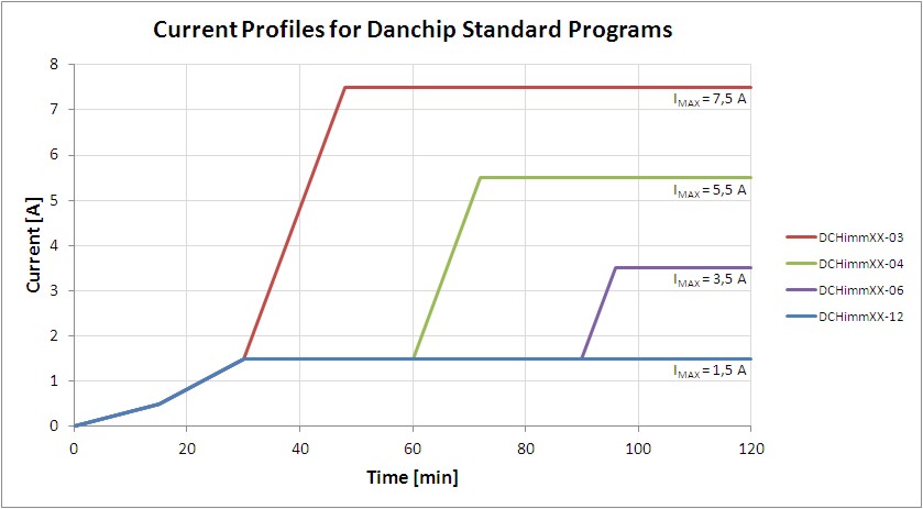
The following figure shows the current profile during the first 2 hours of the programs:

As can be seen from the illustration the first 30 minutes of all standard processes are identical. All processes use a slow ramping of the current. This is to make sure that some material is deposited which can conduct a higher current. Starting a plating process at several amperes is very likely to damage the sample (and possibly the sample holder) because the seed layer (usually 50-120 nm thick) cannot support that high currents.
The Standard programs are named using the following convention: DCHimmXX.X-YY where DCH indicates it's a process developed by Danchip, imm that is a process developed for producing samples for the injection molding machine, XX.X denotes the charge in Ah (Ampere-hours) and YY denotes the approximate process time in hours.
Comparison of standard processes
| DCHimm18.1-03 | DCHimm18.1-04 | DCHimm18.1-06 | DCHimm18.1-12 | |
|---|---|---|---|---|
| Charge [Ah] | 18,1 | 18,1 | 18,1 | 18,1 |
| Expected nickel thickness | 350 µm | 350 µm | 350 µm | 350 µm |
| Maximum current [A] |
7,5 |
5,5 |
3,5 |
1,5 |
| Process time [hh:mm:ss] |
02:58:01 |
04:08:44 |
06:09:26 |
12:20:01 |
| Process comments |
Fastest possible process (maximum allowable current). Will often result in less desirable material properties: high stress levels, high roughness, quite ductile nickel. A perfect seed metal layer and an excellent electrical contact are prerequisites. |
A fast program that allows one to produce two samples in a normal working day. Similar material properties as stated for the 3 hour process, although slightly less 'severe'. |
A compromise between desired material properties (hardness, ductility, roughness) and process time. Will result in a sample that will be useful for most standard injection molding processes. |
A slower process that in return results in lower roughness and stronger mechanical properties. A good choice for shims that will be used with 'harsh' injection molding parameters (high temperatures and high pressures). |
