Specific Process Knowledge/Etch/Etching of Silicon Oxide/SiO2 etch using AOE/Standard recipe with resist mask: Difference between revisions
Jump to navigation
Jump to search
Using different resist masks: results using the standard recipe for "Silicon oxide etch with resist mask"
No edit summary |
No edit summary |
||
| Line 162: | Line 162: | ||
|} | |} | ||
<br clear="all" /> | |||
=Etching of micro structures in Aluminum oxide= | |||
''by Fredrik Stöhr'' | |||
Aluminum oxide (Al<sub>2</sub>O<sub>3</sub>, Alumina) can be etched with the standard recipe for silicon oxide etching. The parameters including the chuck temperature are identical to the recipe described above: '''SiO2_res'''. ''The etch is probably very physical and gives redeposition, so please consider using a Cl2 etch on the ICP metal instead (BGHE 2015-04-17)'' <br> | |||
'''General Description'''<br> | |||
:Process date: Summer 2014<br> | |||
:Aluminum Oxide with a thickness of 50 nm has been deposited by atomic layer deposition using the respective standard recipe.<br> | |||
:Substrates: Blank 525 µm Silicon wafers or Silicon wafers with thermally grown Silicon Oxide prior to Alumina deposition. <br> | |||
:Mask: [XOP8] AZ5214E 1.5 µm thick (HMDS pretreatment, 6-inch aligner 3 sec exposure, 60 sec development). | |||
:Etch Load (Total Exposed SiO2): ~ 5 %<br> | |||
:Post process: O2 Plasma Ashing 10 min | |||
{| border="1" cellspacing="1" cellpadding="1" align="middle" | |||
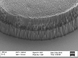
![[image:FRSTO Al2O3 AOE 1 Top 05.jpg|300x300px|thumb|left| | |||
Etch time: 3 min. Substrate: Blank Si. <br> | |||
Bird View. The dark area is Silicon. The bright area is Alumina. The black flakes stem from redeposited sputtered material and is most likely aluminum oxide, since it is almost non-volatile in the used plasma chemistry. It must have been laying on top of the photo resist mask and landed on the alumina after resist ashing. | |||
]] | |||
![[image:FRSTO Al2O3 AOE 2 Top 04.jpg|300x300px|thumb|left| | |||
Etch time: 3 min. Substrate: Blank Si. <br> | |||
Bird View. Close-up. The dark area is Silicon. The bright area is Alumina. The black flakes stem from redeposited sputtered material. | |||
]] | |||
![[image:FRSTO Al2O3 AOE 3 Top Tilt30 08.jpg|300x300px|thumb|left| | |||
Etch time: 3 min. Substrate: Blank Si. <br> | |||
Bird View. Close-up. The dark area is Silicon. The bright area is Alumina. | |||
]] | |||
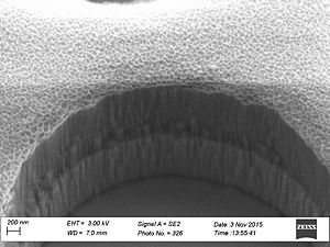
![[image:FRSTO Al2O3 AOE 4 Cross06.jpg|300x300px|thumb|left| | |||
Etch time: 3 min<br> | |||
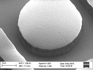
Cross section of deep reactive ion etched silicon (DRIE Pegasus), where the structured alumina was used as a mask. Remarkably, the etch selectivity of Alumina to Silicon is >1:10000. | |||
]] | |||
|- | |||
|} | |||
{| border="1" cellspacing="1" cellpadding="1" align="middle" | |||
![[image:FRSTO Al2O3 AOE 5 Top Tilt30 05.jpg|300x300px|thumb|left| | |||
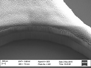
Etch time: 10 min. Substrate: Blank Si. <br> | |||
The view tilt angle is 30°. The edge is corrugated, which is most likely to the corrugated resist mask. | |||
]] | |||
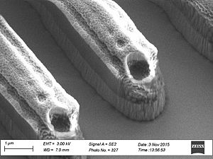
![[image:FRSTO Al2O3 AOE 6 Top Tilt30 04.jpg|300x300px|thumb|left| | |||
Etch time: 10 min. Substrate: Blank Si. <br> | |||
The view tilt angle is 30°. Vertical striations and considerable over-etching of the Silicon substrate are apparent. It seems as if less material has been redeposited, which may be due to the prolonged etch time in comparison to the above. | |||
]] | |||
![[image:FRSTO Al2O3 AOE 7 Top Tilt30 01.jpg|300x300px|thumb|left| | |||
Etch time: 10 min. Substrate: Blank Si. <br> | |||
The view tilt angle is 30°. Vertical striations and considerable over-etching of the Silicon substrate are apparent. It seems as if less material has been redeposited, which may be due to the prolonged etch time in comparison to the above. | |||
]] | |||
|- | |||
|} | |||
{| border="1" cellspacing="1" cellpadding="1" align="middle" | |||
![[image:FRSTO Al2O3 AOE 8 AOE15min Top Tilt45 21.jpg|300x300px|thumb|left| | |||
Etch time: 15 min. Substrate: Silicon with 1 µm thermally grown SiO2 <br> | |||
The view tilt angle is 45°. Alumina and Silicon Oxide may be etched in one go. | |||
]] | |||
![[image:FRSTO Al2O3 AOE 9 AOE15min Top Tilt45 27.jpg|300x300px|thumb|left| | |||
Etch time: 15 min. Substrate: Silicon with 1 µm thermally grown SiO2 <br> | |||
The view tilt angle is 45°. Alumina and Silicon Oxide may be etched in one go. Considerable over-etchign of the Silicon substrate is apparent. | |||
]] | |||
![[image:FRSTO Al2O3 AOE 10 AOE15min Top Tilt45 31.jpg|300x300px|thumb|left| | |||
Etch time: 15 min. Substrate: Silicon with 1 µm thermally grown SiO2 <br> | |||
The view tilt angle is 45°. Alumina and Silicon Oxide may be etched in one go. Considerable over-etchign of the Silicon substrate is apparent. | |||
]] | |||
|- | |||
|} | |||
<br clear="all" /> | <br clear="all" /> | ||
Revision as of 10:27, 24 November 2015
The standard recipe
The standard recipe for oxide etching with photo resist as masking material is called: SiO2_res. The parameters and results so fare are as follows:
| Parameter | Recipe name: SiO2_res (SiO2 etch with resist mask) | Variations over SiO2_res made in 2010 by BGHE |
|---|---|---|
| Coil Power [W] | 1300 | 1000-1600 |
| Platen Power [W] | 200 | 150-300 |
| Platen temperature [oC] | 0 | 0 |
| He flow [sccm] | 174 | 174, 300 |
| C4F8 flow [sccm] | 5 | 5 |
| H2 flow [sccm] | 4 | 0, 4 |
| Pressure [mTorr] | 4 | 2.3, 4 |
Etch rates in different materials using the standard "Silicon oxide etch with resist mask"
| Material to be etched | Etch rate using SiO2_res | |
|---|---|---|
| Thermal oxide | ~230nm/min (5% etch load) - etch load dependency see here | |
| TEOS oxide (5% load) | 233nm/min ±0.7% - "±" represents the non-uniformity over a 100mm wafer - etched in Marts 2013 by LN/BGE@danchip | |
| PECVD1 (standard) oxide (5% load) | 242nm/min ±0.6% - "±" represents the non-uniformity over a 100mm wafer - etched in Marts 2013 by LN/BGE@danchip | |
| Al2O from the ALD | 50nm can be etched in 10min - etched in November 2014 by FRSTO@danchip | |
| Silicon rich nitride from furnace B2 | 136nm was etched in 1min (whole wafer) - etched in October 2015 by bghe@danchip |
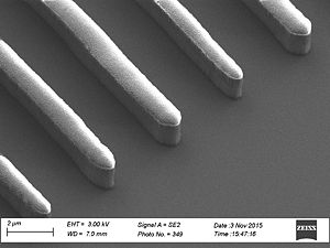
Using different resist masks: results using the standard recipe for "Silicon oxide etch with resist mask" 

| . | Az | MIR | nLof | KRF | CSAR |
|---|---|---|---|---|---|
| Selectivity to thermal oxide [:1] |
|
1.8 - tested November 2015 by BGHE | 2.0 - tested November 2015 by BGHE | ~2 - tested May 2013 by Christian Østergaard @nanotech. | . |
| Profile [o] | ~90 | . | . | . | . |
| Roughness of the resist after etch - striation on sidewalls | . | . | . | . | . |
| Images | See here | . | . | See images here | . |
| Comments | A negative resist process was done to make the mask. I have not had so good results with a positive resist process. | . | . | . | Using the standard oxide recipe (SiO2_res) for 1 min the CSAR looked burned and could not be removed by CSAR stripper (AR600-71). For a better recipe look here |
Striation: Side wall roughness
- Striation with different resists used
Az resist
Az resist
Az resist
Az resist - profile after etch
Mir resist

Mir resist
Mir resist
Mir resist - profile after etch
nLof
nLof
nLof
nLof resist - profile after etch


Variations over the standard "SiO2 etch with resist mask" recipe
| Typical results | Variations over SiO2_res made in 2010 by BGHE See results here |
|---|---|
| Etch rate of thermal oxide | ~160-340nm/min |
| Selectivity to AZ resist [:1] | 2.7-4.3 |
| Profile angle | 83-90 |
| Images | See here |
| Comments | . |
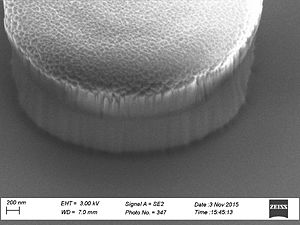
Etching of micro structures in Aluminum oxide
by Fredrik Stöhr
Aluminum oxide (Al2O3, Alumina) can be etched with the standard recipe for silicon oxide etching. The parameters including the chuck temperature are identical to the recipe described above: SiO2_res. The etch is probably very physical and gives redeposition, so please consider using a Cl2 etch on the ICP metal instead (BGHE 2015-04-17)
General Description
- Process date: Summer 2014
- Aluminum Oxide with a thickness of 50 nm has been deposited by atomic layer deposition using the respective standard recipe.
- Substrates: Blank 525 µm Silicon wafers or Silicon wafers with thermally grown Silicon Oxide prior to Alumina deposition.
- Mask: [XOP8] AZ5214E 1.5 µm thick (HMDS pretreatment, 6-inch aligner 3 sec exposure, 60 sec development).
- Etch Load (Total Exposed SiO2): ~ 5 %
- Post process: O2 Plasma Ashing 10 min
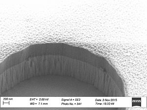
 Etch time: 3 min. Substrate: Blank Si. Bird View. The dark area is Silicon. The bright area is Alumina. The black flakes stem from redeposited sputtered material and is most likely aluminum oxide, since it is almost non-volatile in the used plasma chemistry. It must have been laying on top of the photo resist mask and landed on the alumina after resist ashing. |
|---|


