Specific Process Knowledge/Etch/Etching of Silicon Oxide/SiO2 etch using AOE/Standard recipe with resist mask: Difference between revisions
Jump to navigation
Jump to search
Using different resist masks: results using the standard recipe for "Silicon oxide etch with resist mask"
No edit summary |
No edit summary |
||
| Line 1: | Line 1: | ||
==The standard recipe== | |||
'''The standard recipe for oxide etching with photo resist as masking material is called: SiO2_res. The parameters and results so fare are as follows:''' | '''The standard recipe for oxide etching with photo resist as masking material is called: SiO2_res. The parameters and results so fare are as follows:''' | ||
{| border="1" cellspacing="2" cellpadding="2" | {| border="1" cellspacing="2" cellpadding="2" | ||
Revision as of 12:57, 19 November 2015
The standard recipe
The standard recipe for oxide etching with photo resist as masking material is called: SiO2_res. The parameters and results so fare are as follows:
| Parameter | Recipe name: SiO2_res (SiO2 etch with resist mask) | Variations over SiO2_res made in 2010 by BGHE |
|---|---|---|
| Coil Power [W] | 1300 | 1000-1600 |
| Platen Power [W] | 200 | 150-300 |
| Platen temperature [oC] | 0 | 0 |
| He flow [sccm] | 174 | 174, 300 |
| C4F8 flow [sccm] | 5 | 5 |
| H2 flow [sccm] | 4 | 0, 4 |
| Pressure [mTorr] | 4 | 2.3, 4 |
Etch rates in different materials using the standard "Silicon oxide etch with resist mask"
| Material to be etched | Etch rate using SiO2_res | |
|---|---|---|
| Thermal oxide | ~230nm/min (5% etch load) - etch load dependency see here | |
| TEOS oxide (5% load) | 233nm/min ±0.7% - "±" represents the non-uniformity over a 100mm wafer - etched in Marts 2013 by LN/BGE@danchip | |
| PECVD1 (standard) oxide (5% load) | 242nm/min ±0.6% - "±" represents the non-uniformity over a 100mm wafer - etched in Marts 2013 by LN/BGE@danchip | |
| Al2O from the ALD | 50nm can be etched in 10min - etched in November 2014 by FRSTO@danchip | |
| Silicon rich nitride from furnace B2 | 136nm was etched in 1min (whole wafer) - etched in October 2015 by bghe@danchip |
Using different resist masks: results using the standard recipe for "Silicon oxide etch with resist mask" 

| . | Az | MIR | nLof | KRF | CSAR |
|---|---|---|---|---|---|
| Selectivity to thermal oxide [:1] |
|
1.8 - tested November 2015 by BGHE | 2.0 - tested November 2015 by BGHE | ~2 - tested May 2013 by Christian Østergaard @nanotech. | . |
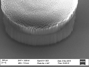
| Profile [o] | ~90 | . | . | . | . |
| Roughness of the resist after etch - striation on sidewalls | . | . | . | . | . |
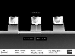
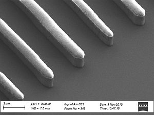
| Images | See here | . | . | See images here | . |
| Comments | A negative resist process was done to make the mask. I have not had so good results with a positive resist process. | . | . | . | Using the standard oxide recipe (SiO2_res) for 1 min the CSAR looked burned and could not be removed by CSAR stripper (AR600-71). For a better recipe look here |
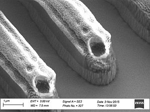
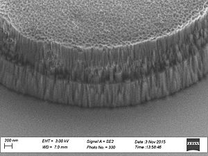
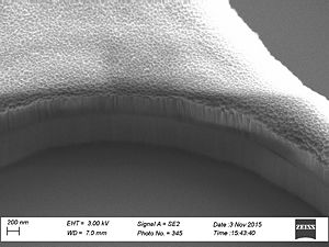
Striation: Side wall roughness
- Striation with different resists used
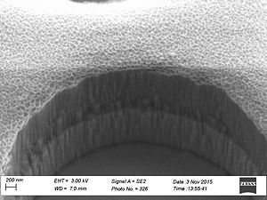
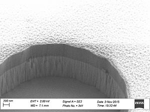
Az resist
Az resist
Az resist
Az resist - profile after etch
Mir resist

Mir resist
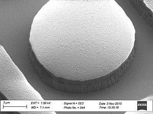
Mir resist
Mir resist - profile after etch
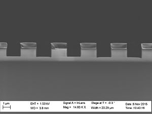
nLof
nLof
nLof
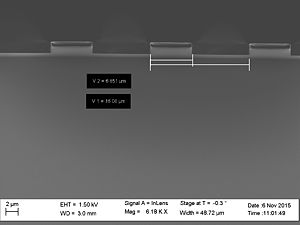
nLof resist - profile after etch


Variations over the standard "SiO2 etch with resist mask" recipe
| Typical results | Variations over SiO2_res made in 2010 by BGHE See results here |
|---|---|
| Etch rate of thermal oxide | ~160-340nm/min |
| Selectivity to AZ resist [:1] | 2.7-4.3 |
| Profile angle | 83-90 |
| Images | See here |
| Comments | . |