Specific Process Knowledge/Characterization/SEM LEO: Difference between revisions
| Line 24: | Line 24: | ||
*[[/SEM comparison tablel|SEM comparison table]] | *[[/SEM comparison tablel|SEM comparison table]] | ||
| Line 31: | Line 32: | ||
!colspan="2" border="none" style="background:silver; color:black;" align="center"|Equipment | !colspan="2" border="none" style="background:silver; color:black;" align="center"|Equipment | ||
|style="background:WhiteSmoke; color:black"|<b> | |style="background:WhiteSmoke; color:black"|<b>SEM LEO (Leo 1550 SEM)</b> | ||
|- | |- | ||
!style="background:silver; color:black;" align="center" width="60"|Purpose | !style="background:silver; color:black;" align="center" width="60"|Purpose | ||
|style="background:LightGrey; color:black"| | |style="background:LightGrey; color:black"|Imaging and measurement of | ||
|style="background:WhiteSmoke; color:black"| | |||
*Any (semi)conducting sample that may have thin (> ~ 5 µm) layers of non-conducting materials on top | |||
|- | |||
!style="background:silver; color:black;" align="center" width="60"|Location | |||
|style="background:LightGrey; color:black"| | |||
|style="background:WhiteSmoke; color:black"| | |||
*Cleanroom of DTU Danchip | |||
|- | |||
!style="background:silver; color:black;" align="center" width="60"|Performance | |||
|style="background:LightGrey; color:black"|Resolution | |||
|style="background:WhiteSmoke; color:black"| | |||
*~ 5 nanometers (limited by vibrations) | |||
The resolution is strongly dependent on the type of sample and the skills of the operator. | |||
|- | |||
!style="background:silver; color:black" align="center" valign="center" rowspan="5"|Instrument specifics | |||
|style="background:LightGrey; color:black"|Detectors | |||
|style="background:WhiteSmoke; color:black"| | |style="background:WhiteSmoke; color:black"| | ||
* | *Secondary electron (Se2) | ||
* | *Inlens secondary electron (Inlens) | ||
* | *Backscatter electron (BSD) | ||
|- | |- | ||
|style="background:LightGrey; color:black"|Stage | |||
|style="background:LightGrey; color:black"| | |||
|style="background:WhiteSmoke; color:black"| | |style="background:WhiteSmoke; color:black"| | ||
* | *X, Y: 125 × 100 mm | ||
* | *T: 0 to 90o | ||
* | *R: 360o | ||
*Z: 48 mm | |||
|- | |- | ||
|style="background:LightGrey; color:black"| | |style="background:LightGrey; color:black"|Electron source | ||
|style="background:WhiteSmoke; color:black"| | |style="background:WhiteSmoke; color:black"| | ||
* | *FEG (Field Emission Gun) source | ||
|- | |- | ||
|style="background:LightGrey; color:black"|Operating pressures | |||
|style="background:LightGrey; color:black"| | |||
|style="background:WhiteSmoke; color:black"| | |style="background:WhiteSmoke; color:black"| | ||
* | *Fixed at High vacuum (2 × 10⁻⁵mbar - 10-6mbar) | ||
|- | |- | ||
|style="background:LightGrey; color:black"| | |style="background:LightGrey; color:black"|Options | ||
|style="background:WhiteSmoke; color:black"| | |style="background:WhiteSmoke; color:black"| | ||
* | *Raith Elphy Quantum E-Beam Litography system | ||
|- | |- | ||
!style="background:silver; color:black" align="center" valign="center" rowspan="3"|Substrates | !style="background:silver; color:black" align="center" valign="center" rowspan="3"|Substrates | ||
|style="background:LightGrey; color:black"|Batch size | |style="background:LightGrey; color:black"|Batch size | ||
|style="background:WhiteSmoke; color:black"| | |style="background:WhiteSmoke; color:black"| | ||
*1 | *1 100 mm wafer | ||
*1 | *1 150 mm wafer (not full view) | ||
* | *Smaller samples | ||
|- | |- | ||
| style="background:LightGrey; color:black"|Allowed materials | | style="background:LightGrey; color:black"|Allowed materials | ||
|style="background:WhiteSmoke; color:black"| | |style="background:WhiteSmoke; color:black"| | ||
* | *Any standard cleanroom materials. | ||
Use dedicated samples holders for samples from Black Magic PECVD | |||
|- | |- | ||
|} | |} | ||
Revision as of 15:40, 9 November 2015
THIS PAGE IS UNDER CONSTRUCTION
Feedback to this page: click here
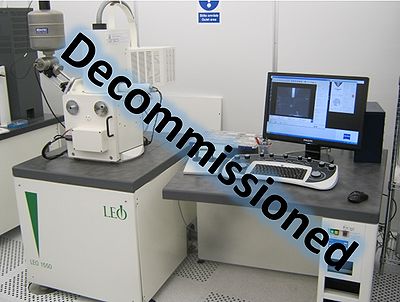
SEM LEO
A Danchip there are five scanning electron microscopes (SEMs). These SEMs cover a wide range of needs both in the cleanroom and outside: From the fast in-process verification of different process parameters such as etch rates, step coverages or lift-off quality to the ultra high resolution images on any type of sample intended for publication.
The SEM LEO was installed in the cleanroom in the 1998, and the software was ungraded in 2012.
This SEM will cover most users need. It is a very reliable and rugged instrument that provides high quality images of most samples. Excellent images on a large variety of materials such as semiconductors, semiconductor oxides or nitrides, metals, thin films and some polymers may be acquired on the SEM.
The SEM is is equipped with a Raith e-beam writing system. This system requires a special training.
The user manual, control instruction, the user APV and contact information can be found in LabManager:
SEM LEO info page in LabManager,
Performance information
| Equipment | SEM LEO (Leo 1550 SEM) | |
|---|---|---|
| Purpose | Imaging and measurement of |
|
| Location |
| |
| Performance | Resolution |
The resolution is strongly dependent on the type of sample and the skills of the operator. |
| Instrument specifics | Detectors |
|
| Stage |
| |
| Electron source |
| |
| Operating pressures |
| |
| Options |
| |
| Substrates | Batch size |
|
| Allowed materials |
Use dedicated samples holders for samples from Black Magic PECVD | |
