Specific Process Knowledge/Characterization/Element analysis: Difference between revisions
| Line 9: | Line 9: | ||
* SIMS | * SIMS | ||
* XPS (ESCA) | * XPS (ESCA) | ||
Revision as of 10:52, 31 August 2015
Feedback to this page: click here
Element analysis at Danchip
The following techniques for elemental analysis are available at Danchip.
- EDX
- SIMS
- XPS (ESCA)
You can make detailed analysis on the elemental composition and distribution in a sample with 4 instruments at Danchip. The
Leo SEM and
FEI SEM are both equipped with an X-ray detector that allows you to make elemental analysis by using the technique Energy Dispersive X-ray analysis or EDX. The
Atomika SIMS uses a technique called Secondary Ion Mass Spectrometry or SIMS. The
XPS-ThermoScientific can be used for X-ray Photoelectron Spectroscopy measurements.
Comparison of EDX, SIMS and XPS
| SEM with EDX | SIMS | XPS | |
|---|---|---|---|
| Full name | Energy Dispersive X-ray Analysis | Secondary Ion Mass Spectroscopy | X-ray Photoelectron Spectroscopy |
| Technique | Non destructive method: X-rays are generated when the primary beam impinges on the sample. The elemental analysis is possible because the energy of these X-rays is characteristic of the element they emitted from. | Destructive method: A beam of high energy heavy ions (caesium or oxygen) sputters off surface atoms that are subsequently measured with a mass spectrometer. | Non destrucive method: X-rays are irridiating the sample, and the energy of edjected photoelectrons is measured. The elemental analysis is possible, since the binding energy of the electrons (and hence the energy of the emitted photoelectrons) are specific for each element. |
| What elements are detected | Every element heavier than boron/carbon | Every element | Every element except hydrogen and helium. However, the signal from two substances can overlapp, which can reduce the detection limit |
| Chemical information | None: Only transistions involving inner shell electrons are detected | None | Chemical state information |
| Sample limitations | Vacuum compatible. | Vacuum compatible. The sample needs to be cut into small (app. 5*5 mm) pieces. | Vacuum compatible. Sample size max 50x50 mm, thickness max 20 mm. |
| Spatial resolution | Very precise point-like analysis is possible with SEM electron beam. | Limited to what is visible in a camera | Limited to what is visible in a camera |
| Depth resolution | The size interaction volume depends on the SEM high voltage and sample density: The higher the SEM high voltage the bigger and deeper the interaction volume. The more dense the material is the smaller is the interaction volume. See section 'Spatial resolution using EDX' below. | The sputtering of the surface makes it possible to perform detailed depth profiling with extremely good sensitivity and depth resolution. | Very surface sensitive technique. Signal only from the top layer (a few nanometers deep) can be detected. By using the ion beam etch, the composition of deeper lying layers can be probed. |
| Detection limit | Approximately 1 % atomic weight | Down to 1 ppb for many elements | Approximately 1 % atomic weight |
| Speed of measurement | Quite fast and easy | Time consuming | Quite fast and easy |
Energy Dispersive X-ray analysis (EDX)
The technique of extracting information from the X-rays generated in a sample that is irradiated with electrons is called energy dispersive X-ray analysis or EDX. (Other acronyms are Energy Dispersive x-ray Spectroscopy, EDS, or Electron Probe Microanalysis, EPMA). The energetic electrons in the incident beam create core level vacancies as they collide with sample atoms electrons in a multiple scattering process. This leaves the atoms in the sample in an excited state. In the process of decaying from this state photons may be emitted. The energy of these photons is determined by the difference in energy of the shells involved. Since atomic shells are unique for every element so will be the transitions between them. Thus, every element has its own characteristic X-ray spectrum that can be used to determine the elemental composition.
Adding an EDX detector to a SEM provides a very powerful tool for elemental analysis. The capability of the SEM to precisely maneuver the electron beam in a number of ways enables us to make point-like analysis with nanometer precision.
- The techniques EDX, SIMS and XPS
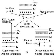
The high energy electrons in the beam (denoted above as incident particle) collide with the core electrons of the sample atoms that are left in an excited state with higher energy. One decay mechanism is to let an outer electron fall into the unoccupied state under emission of a photon that carries the excess energy. This energy is determined by the electronic shells and hence characteristic of the atom.
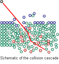
A beam of high energy ions is rastered on the surface of the sample. Some of the atoms that used to make up the surface are sputtered off and emitted as secondary ions. The mass of the these ions is measured with a mass spectrometer.
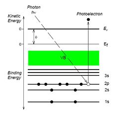
The atoms in the sample is irradiated with X-rays and the energy of the incoming photons are adsorbed. Photoelectrons are ejected, and the energy of these electrons can be measured. Since the energy of the incoming photon is known, the binding energy of the electrons in the atom can be determined. The binding energy is characteristic for the element, and therefore the composition of the sample can be determined.


Spatial resolution using EDX
Using the the very fine beam of electrons from a SEM one is capable of making point-like elemental analysis of the sample. A multiple scattering process will occur when the incident electrons collide with the sample electrons. This process generates low energetic secondary electrons and it continues until the incident electrons have lost so much energy that they are not different from the secondary electrons. The volume of the sample inside which this process takes place is called the interaction volume. X-rays are generated throughout the interaction volume and we are therefore probing the whole volume when using the EDX detector.
Using some empirical equations one can calculate how the distribution of X-rays generated in the sample will be at certain high voltages. Below are shown the depth profiles of X-rays from silicon and gold when irradiated with 5-30 kV electrons.
- Curves that show the depth of origin of the X-rays
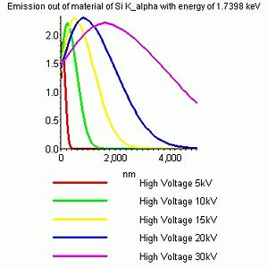
The depth profiles of X-rays emerging from bulk silicon at different high voltages.
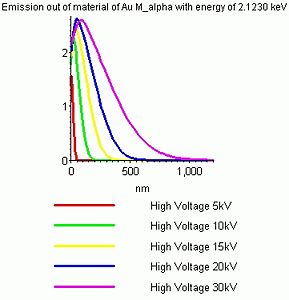
The depth profiles of X-rays emerging from bulk gold at different high voltages.


It is seen that the trend is:
- Increasing the high voltage gives rise to a bigger and deeper interaction volume and hence increases the depth which is probed.
- Increasing the density of the sample material reduces the size and depth of the interaction volume - hence a more shallow layer is probed.
Secondary Ion Mass Spectrometry (SIMS)
In the Atomika SIMS the samples are bombarded with a beam of either oxygen or caesium ions. When accelerated to high energy and rastered across the sample these ions will be able to gradually sputter off the surface atoms in a small area defined by the raster pattern. Some of the surface atoms are emitted as ionized particles. In this way one layer after another is peeled off the sample.
These charged species are led through a mass spectrometer where a magnetic field is used to deflect them. The deflection increases with charge and decreases with mass and we are therefore able detect and count them according to their mass. This technique is called Secondary Ion Mass Spectrometry or SIMS.
Typical application of SIMS
SIMS is the most sensitive technique for elemental composition. It is therefore ideal if you want to check doping profiles or for contaminations.
A typical application would be to check the concentration profile of boron doping in silicon. In that case one would put two samples into the SIMS.
- A reference sample with a known boron profile
- A sample
X-ray Photoelectron Spectroscopy analysis (XPS)
During a XPS (X-ray Photoelectron Spectroscopy) analysis, the sample is irradiated with photons of a specific energy (in the Danchip system 1486 eV). When energy of the irradiating X-rays is adsorbed by the atoms in the sample, photoelectrons are ejected [[1]].
Since the energy of the incoming photons is known, and the energy of the ejected electrons is measured, the binding energy of the electrons in the probed atoms can be determined. The binding energy of the electrons are element specific, and is therefore a "finger-print" of the atom. Hence, a measurement of the XPS spectrum gives information of which materials are present in the sample, and at which concentrations.
XPS is an excellent technique to probe the chemical state of atoms on a surface. The binding energy of lower lying atomic levels (for example 1s, 2s and 2p) are at a specific energy, but is slightly affected by the chemical environment of the probed atom. This is known as the chemical shift. By measuring the shift of the electron binding energies one can determined the chemical state of atoms. See an example on the page XPS-ThermoScientific.
Typical applications of XPS
The XPS can be used for different applications, for example:
- Do an elemental analysis of the outermost layer of your surface.
- Check the composition of a film at different depths.
- Check for a contaminations.
- It not as sensitive as the SIMS, but faster, so it can be an alternative if you are checking for a bit higher contamination levels (like 1 %)
- Do a analysis of the chemical state of atoms present on the surface.
- See what effect a surface treatment of your sample has on the surface chemistry.
- Check a polymer covered surface. Are for example (C=O), (C-OH) (C-C) groups present in the polymer after it been deposited on a surface.