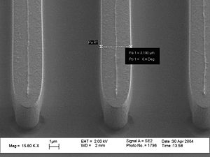
Specific Process Knowledge/Etch/Etching of Silicon Oxide/SiO2 etch using RIE1 or RIE2/Images of 1SIO2mbr with burned resist mask: Difference between revisions
Jump to navigation
Jump to search
(New page: ===Etch of SiO2 using the recipe 1SIO2mbr with burned resist as masking material, by Berit Geilman Herstrøm (BGE) from Danchip@DTU=== {| border="2" cellspacing="1" cellpadding="3" align=...) |
No edit summary |
||
| Line 1: | Line 1: | ||
'''Feedback to this page''': '''[mailto:labadviser@danchip.dtu.dk?Subject=Feed%20back%20from%20page%20http://labadviser.danchip.dtu.dk/index.php/Specific_Process_Knowledge/Etch/Etching_of_Silicon_Oxide/SiO2_etch_using_RIE1_or_RIE2/Images_of_1SIO2mbr_with_burned_resist_mask click here]''' | |||
===Etch of SiO2 using the recipe 1SIO2mbr with burned resist as masking material, by Berit Geilman Herstrøm (BGE) from Danchip@DTU=== | ===Etch of SiO2 using the recipe 1SIO2mbr with burned resist as masking material, by Berit Geilman Herstrøm (BGE) from Danchip@DTU=== | ||
Revision as of 11:01, 28 May 2015
Feedback to this page: click here
