Specific Process Knowledge/Etch/IBE⁄IBSD Ionfab 300/IBE blazed gratings: Difference between revisions
No edit summary |
No edit summary |
||
| Line 1: | Line 1: | ||
'''Feedback to this page''': '''[mailto:labadviser@danchip.dtu.dk?Subject=Feed%20back%20from%20page%20http://labadviser.danchip.dtu.dk/index.php/Specific_Process_Knowledge/Etch/IBE⁄IBSD_Ionfab_300/IBE_blazed_gratings click here]''' | '''Feedback to this page''': '''[mailto:labadviser@danchip.dtu.dk?Subject=Feed%20back%20from%20page%20http://labadviser.danchip.dtu.dk/index.php/Specific_Process_Knowledge/Etch/IBE⁄IBSD_Ionfab_300/IBE_blazed_gratings click here]''' | ||
''by bghe@danchip'' | ''by bghe@danchip'' | ||
<gallery caption="Some examples of blazed gratingens in fused silica etched with Cr and DUV resist as masking layer " widths="300px" heights="250px"> | <gallery caption="Some examples of blazed gratingens in fused silica etched with Cr and DUV resist as masking layer " widths="300px" heights="250px"> | ||
Revision as of 10:35, 27 May 2015
Feedback to this page: click here
by bghe@danchip
- Some examples of blazed gratingens in fused silica etched with Cr and DUV resist as masking layer
-
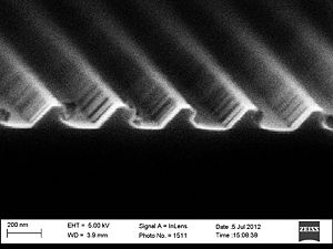 30min etch with 100nm Cr mask, used recipe BGHE blazed gratings with CHF3
*Rotation speed 0 rpm
*Angle: -35
*I(N)=400mA
*RF power=1300W
*I(B)=300mA
*V(B)=300V
*V(AC,B)=500V
*Ar(N) flow=5sccm
*Ar(B) flow=5sccm
*CHF3 flow=15sccm -
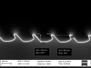 45min etch with 100nm Cr mask, used recipe BGHE blazed gratings with CHF3
*Rotation speed 0 rpm
*Angle: -35
*I(N)=400mA
*RF power=1300W
*I(B)=300mA
*V(B)=300V
*V(AC,B)=500V
*Ar(N) flow=5sccm
*Ar(B) flow=5sccm
*CHF3 flow=15sccm -
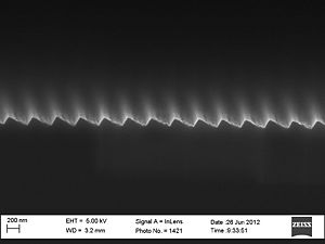 20min etch with Krf resist, all resist is gone, used recipe BGHE blazed gratings
*Rotation speed 0 rpm
*Angle: -35
*I(N)=550mA
*RF power=1300W
*I(B)=500mA
*V(B)=600V
*V(AC,B)=400V
*Ar(N) flow=5sccm
*Ar(B) flow=10sccm
*CHF3 flow=0sccm -
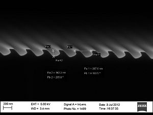 15+30min etch with 50nm Cr mask, used recipe BGHE blazed gratings with CHF3
*Rotation speed 0 rpm
*Angle: -35
*I(N)=400mA
*RF power=1300W
*I(B)=300mA
*V(B)=300V
*V(AC,B)=500V
*Ar(N) flow=5sccm
*Ar(B) flow=5sccm
*CHF3 flow=15sccm


