Specific Process Knowledge/Etch/ICP Metal Etcher/silicon/nano/nanoetch/180nmzep: Difference between revisions
< Specific Process Knowledge | Etch | ICP Metal Etcher | silicon | nano
Jump to navigation
Jump to search
(Created page with "<gallery caption="The profiles of the 180 nm zep resist" widths="250" heights="200" perrow="3"> image:WF_2B1_feb06_2011-030.jpg|The 30 nm zep profile image:WF_2B1_feb06_2011-0...") |
No edit summary |
||
| Line 1: | Line 1: | ||
'''Feedback to this page''': '''[mailto:labadviser@danchip.dtu.dk?Subject=Feed%20back%20from%20page%20http://labadviser.danchip.dtu.dk/index.php/Specific_Process_Knowledge/Etch/ICP_Metal_Etcher/silicon/nano/nanoetch/180nmzep click here]''' | |||
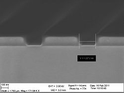
<gallery caption="The profiles of the 180 nm zep resist" widths="250" heights="200" perrow="3"> | <gallery caption="The profiles of the 180 nm zep resist" widths="250" heights="200" perrow="3"> | ||
image:WF_2B1_feb06_2011-030.jpg|The 30 nm zep profile | image:WF_2B1_feb06_2011-030.jpg|The 30 nm zep profile | ||
Revision as of 12:12, 22 October 2013
Feedback to this page: click here
- The profiles of the 180 nm zep resist
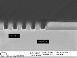
The 30 nm zep profile
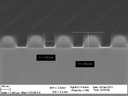
The 60 nm zep profile
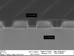
The 90 nm zep profile
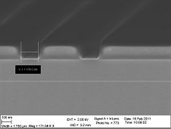
The 120 nm zep profile
The 150 nm zep profile


