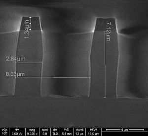
Specific Process Knowledge/Etch/Etching of Silicon Oxide/SiO2 etch using AOE/PolySi mask/Images of AOEpsiB 8

From LabAdviser
< Specific Process Knowledge‎ | Etch‎ | Etching of Silicon Oxide‎ | SiO2 etch using AOE‎ | PolySi mask
Revision as of 12:50, 3 February 2023 by Bghe (talk | contribs)
(diff) ← Older revision | Latest revision (diff) | Newer revision → (diff)
Jump to navigation Jump to search

Feedback to this page: click here
This page is written by Berit Herstrøm @ DTU Nanolab (BGHE) if nothing else is stated
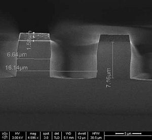
Process date: 25. July 2012 by bghe@nanolab
Recipe: low line width reduction
Process time: 30 min
Mask: Poly Si 2.2 µm thick
Etch depth: 7.2 µm
Line width mask: 8µm
Line with after etch: 6.6µm
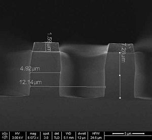
Process date: 25. July 2012 by bghe@nanolab
Recipe: low line width reduction
Process time: 30 min
Mask: Poly Si 2.2 µm
Etch depth: 7.3 µm
Line width mask: 6µm
Line with after etch: 4.9µm
Process date: 25. July 2012 by bghe@nanolab
Recipe: low line width reduction
Process time: 30 min
Mask: Poly Si 2.2 µm
Etch depth: 7.1 µm
Line width mask: 4µm
Line with after etch: 2.8µm