Unless anything else is stated, everything on this page, text and pictures are made by DTU Nanolab.
All links to Kemibrug (SDS) and Labmanager Including APV and QC requires login.
Feedback to this page: click here
Comparing silicon oxide etch methods at DTU Nanolab
There are a broad varity of silicon oxide etch methods at DTU Nanolab. The methodes are compared here to make it easier for you to compare and choose the one that suits your needs.
Compare the methods for Silicon Oxide etching
|
|
Wet Silicon Oxide etch (BHF/HF)
|
ASE
|
III-V RIE
|
AOE (Advanced Oxide Etch)
|
DRIE Pegasus 4
|
ICP metal
|
IBE/IBSD Ionfab 300
|
HF Vapour Phase Etch
|
| Generel description
|
|
- Anisotropic etch: vertical sidewalls
|
- Anisotropic etch: vertical sidewalls
- Premarily for III-V samples
|
- Anisotropic etch: vertical sidewalls
|
- Anisotropic etch: almost vertical sidewalls
|
- Anisotropic etch: almost vertical sidewalls
- We prefer that SiO2 etch takes place in the AOE or Pegasus 4.
|
- Primarily for pure physical etch by sputtering with Ar-ions
|
- Gas phase HF etching with ethanol as carrier
|
| Possible masking materials
|
- Photoresist
- PolySilicon
- Silicon nitride (LPCVD)
- Blue film
- Cr/Au for deeper etches (plastic beaker)
|
- Photoresist
- DUV resist
- E-beam resist
- Silicon
- Silicon Nitride
- Metals if they cover less than 5% of the wafer area
|
- Photoresist
- DUV resist
- E-beam resist
- Aluminum
- Silicon
- Silicon Nitride
|
- Photoresist
- DUV resist
- E-beam resist
- Silicon
- Silicon Nitride
- Aluminium
- Chromium (Please try to avoid this)
|
- Photoresist
- DUV resist
- E-beam resist
- Si
- Silicon Nitride
- Chromium (ask for permission)
|
- Photoresist
- DUV resist
- E-beam resist
- Si
- Silicon Nitride
- Aluminium
- Chromium
|
- Any material that is accepted in the machine
|
- Aluminium
- Aluminium oxide
- Polysilicon
|
| Etch rate range
|
- ~75 nm/min (Thermal oxide) in BHF
- ~80 nm/min (Thermal oxide) in BOE 7:1 Etchant VLSI with Surfactant
- ~25 nm/min (Thermal oxide) in 5%HF
- ~6 nm/min (Thermal oxide) in 1%HF
- ~3-4µm/min in 40%HF
|
- Process dependent
- Tested range: ~20nm/min - ~250nm/min
|
- Process dependent
- Tested range: ~1nm/min - ~30nm/min
|
- Process dependent
- Tested range: ~60nm/min - ~550nm/min
|
<500nm/min
|
- Process dependent
- Tested range: ~40nm/min - ~200nm/min
|
- Process dependent
- Tested once ~22nm/min
|
- Sample and load dependent
- Expected range: 12 - 175 nm/min
|
| Substrate size
|
- #1-25 100mm wafers in our 100mm bath
- What can be fitted in a plastic beaker
|
- As many small samples as can be fitted on the 100mm carrier (bad/no cooling!).
- #1 100mm wafer (or smaller with carrier)
- #1 150mm wafer (only when set up for 150mm)
|
|
- As many small samples as can be fitted on a 100mm wafer
- #1 50 mm wafer fitted on a 100mm wafer
- #1 100 mm wafer
- #1 150 mm wafers (only when the system is set up to 150mm)
|
- As many small samples as can be bonded on a 150mm wafer
- #1 50 mm wafer bonded on a 150mm wafer
- #1 100 mm wafer bonded on a 150nm wafer
- #1 150 mm wafers
|
- As many small samples as can be fitted on a 150mm wafer
- #1 50 mm wafer fittesd on a 150mm wafer
- #1 100 mm wafer fitted on a 150nm wafer
- #1 150 mm wafers
|
- As many samples as can be securely fitted on a up to 200mm wafer
- #1 50 mm wafer with special carrier
- #1 100 mm wafer with special carrier
- #1 150 mm wafers with special carrier
- #1 200 mm wafer
|
- Pieces
- #1 50 mm wafer
- #1 100 mm wafer
- #1 150 mm wafer
|
| Allowed materials
|
In the dedicated bath:
- Silicon
- Silicon Oxide
- Silicon Nitride
- Silicon Oxynitride
- Photoresist
- Blue film
In a plastic beaker:
- No limits cross contamination wise
|
|
|
|
|
|
|
|
Dry etch with Hard mask
By Martin Lind Ommen - fall 2016
Testing selectivities for SiO2 etching with hard masks on AOE and ICP metal with different recipes.All tests are done with 100% etching load
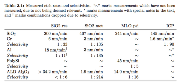
MLO_psi is the version of SiO2_psi on labadviser that is shown under low line with reduction.
The recipe ICP is on ICP metal call: A SiO2 etch with C4F8 with resist mask
I had problems with this recipe - it gave polymer on the surface, therefor I do not have more info on that.
