Specific Process Knowledge/Etch/Wet Silicon Oxide Etch (BHF)
Feedback to this page: click here
Unless anything else is stated, everything on this page, text and pictures are made by DTU Nanolab.
All links to Kemibrug (SDS) and Labmanager Including APV, requires login.
Wet Silicon Oxide Etch (BHF, HF and BOE 7:1 Etchant VLSI with Surfactant (wetting agent))
Silicon oxide can be etched using HF. At DTU Nanolab it is mainly used in a buffered version BHF (premixed). You can find safety datasheets on Kemibrug here The BHF has a more stable etch rate and is more gentle to photoresist due to an almost pH neutral solution which makes photoresist a good masking material for the oxide etch.
BOE 7:1 Etchant VLSI with Surfactant (BHF with wetting agent) can also be used for etching silicon oxide. This is mainly for etching small holes. If you have wetting problems in BHF try the BOE 7:1 Etchant VLSI with Surfactant. It is also a good idea to wet the sample in water for a few minutes before etching.
Wafers with metals or other materials, not allowed in the dedicated oxide etch baths, can be etched using a plastic in Fume hood 01 or 02 (Acids/bases) in D-3. Samples with III-V materials (e.g. InP and GaAs) must be etched in Fume hood 07: III-V Avids/bases in D-3.
The user manual for Oxide etch 1: BHF, APV's and contact information can be found in LabManager by clicking here
The user manual for Oxide etch 2: BHF (clean), APV's and contact information can be found in LabManager by clicking here
The user manual for various HF baths in RCA and Fume hoods, APV's and contact information can be found in LabManager by clicking here
Process information:
See more etch rates in HF solutions.
| Etchant | BHF | 1% HF / 5% HF / 10% HF | 40% HF | BOE 7:1 Etchant VLSI with Surfactant | |
|---|---|---|---|---|---|
| Purpose | Etching of silicon oxide |
|
|
|
|
| Link to safety APV and SDS (You must be logged in to Kemibrug to view SDSs) | |||||
| Performance | Isotropic |
|
|
|
|
| Etch rates |
|
|
|
| |
| Lifetime of photoresist |
|
|
|
| |
| Process parameter range | Chemical solution |
|
|
|
|
| Temperature |
|
|
|
| |
| Substrates | Masking material |
|
|
|
|
Life time of the photoresist and blue film in BHF
Photoresist delaminates from the substrate in BHF. For standard photoresist this process starts after about or less than ½ hour but the time can vary with resist pattern. It starts by under etching the photoresist at the edges. The life time can be prolonged a little to ½ hour - 40 minutes if the photoresist is baked at 120oC.
Blue film also has a limited life time in BHF. Blue film is mainly used for back side protecting the wafer while etching on the front side. The life time of Blue film is also about ½ hour.
- Different places to do wet silicon oxide etch
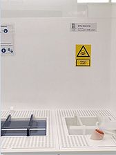
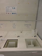
BHF clean wetbench 04 in D-3. Wet silicon oxide etch bath positioned to the right in the wetbench. This bath can also be used for BHF with wetting agent.
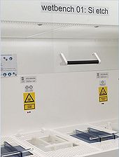
BHF in wetbench 01 Si etch in D-3 (Oxide etch 1: BHF.) The BHF bath is positioned in the middle of the bench. This is primarily used to remove oxide before and after a Si etch.
HF baths in RCA bench in B-1.
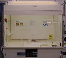
The HF bath in 'Fume hood(RCA)' in cleanroom B-1 is only for use during special RCA cleaning processes inside the fume hood.


Comparing different BHF baths
| BHF (KOH) in D-3(Oxide etch 1: BHF) | BHF clean in D-3 (Oxide etch 2: BHF) | BHF in RCA Bench | BHF in PP-bath | BHF Plastic beaker | |
|---|---|---|---|---|---|
| Batch size! | 1-25 wafers at a time | 1-25 wafer at a time | 1-25 wafers at a time | 1-25 wafers at a time | 1-7 wafers at a time |
| Size of substrate | 2"-6" wafers | 2"-6" wafers | 2"-6" wafers | 2"- 4" wafers or any that fits in a dedicated holder | 2"- 4" wafers or any that fits in a dedicated holder |
| Allowed materials |
|
|
|
|
|
| Restrictions | Wafers have to be cleaned in 7UP or RCA before further processing. | No wafers with metal are allowed in this bath | Only for wafers with phosphor glass or boron glass that comes directly from one of the furnaces in stack A. All other substrates and material are strictly forbidden to go into the tank. | None | None |
Comparing different HF baths
| 1% HF in RCA Bench | 1% HF PP-bath | 1% HF Plastic beaker | |
|---|---|---|---|
| Batch size! | 1-25 wafers at a time | 1-25 wafer at a time | 1-7 wafers at a time |
| Size of substrate | 2"-6" wafers | 2"- 4" wafers or any that fits in a dedicated holder | 2"- 4" wafers or any that fits in a dedicated holder |
| Allowed materials | Only for wafers that are being RCA cleaned | All materials | All materials |
Comparing different 40% HF baths
| 40% HF PP-bath | 40% HF Plastic beaker | |
|---|---|---|
| Batch size! | 1-25 wafers at a time | 1 wafer at a time |
| Size of substrate | Any that fits to a dedicated holder | Any that fits to a dedicated holder |
| Allowed materials | All materials | All materials |
BOE 7:1 Etchant VLSI with Surfactant bath
| BOE 7:1 Etchant VLSI with Surfactant bath | |
|---|---|
| Batch size! | 1-25 wafers at a time |
| Size of substrate | 4" wafers |
| Allowed materials |
|
| Remark |
Amorphous silicon can be used as a mask fro SiO2 etching. |