Specific Process Knowledge/Etch/DryEtchProcessing/Bonding
Feedback to this page: click here
Unless otherwise stated, the content of this page was created by the dry etch group at DTU Nanolab
Carriers for dry etching: Temporary bonding of samples or carriers for none bonded samples
Purpose
The dry etch tools are set up for processing one particular size of wafer. The reasons why a tool processes one size of wafers and not others are numerous - they may include:
- Hardware availability
- Processes required by users
The dry etch tools at Nanolab all have a default wafer size and may have other sizes of electrodes available. Other sizes of wafers or chips may also be processed but they will require the use of a carrier wafer. Using a carrier is also often required if the side of the wafer facing the electrode has structures.
| Tool | Default substrate size | Alternative substrate size(s) | Sizes of wafers or chips that may bonded and processed |
|---|---|---|---|
| DRIE-Pegasus-1 | 4" wafer | 6" wafer | Samples smaller than a 4" wafer |
| DRIE-Pegasus-2 | 6" wafer | 4" wafer | Samples smaller than a 6" wafer |
| ASE | 4" wafer | 6" wafer | Samples smaller than a 4" wafer |
| AOE | 4" wafer | None | Samples smaller than a 4" wafer |
| ICP Metal Etch | 6" wafer | 4" wafer | Samples smaller than a 6" wafer |
| III-V ICP | 4" wafer | None | Samples smaller than a 4" wafer |
Issues to consider
There are several issues to consider when processing a substrate that is lying (either fixed with a bonding material or lying freely) on a carrier.
- Process temperature
- The cooling of a wafer that is lying directly on the electrode is significantly more efficient than if the wafer is lying on top of a carrier. With no bonding material the wafer is essentially only touching the carrier in three points - thus drastically reducing the heat transfer to the electrode. The possible change in substrate temperature may cause the process to drift or the mask to burn away much faster. Using a bonding material such as crystal bond will increase the heat transfer between carrier and substrate.
- Process aggressiveness and material removal
- The chemical etching of materials (for instance if silicon is etched by flourine) releases energy that has to dissipated to the electrode. This release of energy depends on two factors:
- The faster the etch rate is, the more material is removed pr second, hence the more heat needs to be dissipated. This means that high power etches are much more sensible to poor heat transfer than low power processes.
- The larger area of the wafer that is etched, the more material is removed pr second. Hence, wafers with a high density of areas open for etching, will be more sensible to poor heat conductivity than wafers with little opening.
- Plasma uniformity
- The plasma will adapt to the substrate+carrier sandwich and bow along the edges of the substrate potentially disturbing the electric field that directs the ions towards the surface. This non-uniformity can be important if the substrate is very small.
Procedures
Making Carrier with capton(polyimide) tape
If you do not want to bond your sample to the carrier you can make a carrier wafer by adding pieces of capton tape on the carrier wafer to avoid the sample to slide off the carrier inside the chamber. You have to follow this procedure to keep the carrier clean.
file:Making carrier with capton tape.docx
Bonding
- Find a carrier wafer that has the right size. Keep in mind that it matters a great deal if the surface will be etched or not, i.e. if it has oxide or not.
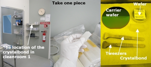
- Take a piece of crystalbond from the shelf in cleanroom A-1.
- Take your items (substrate, carrier wafer, crystalbond and tweezers) to the hotplate in cleanroom C-1.
- Put the carrier wafer on the hotplate.
- Apply a very thin layer of crystalbond in a circular motion so that it covers some 70 % of the area to be covered by your substrate. Do not apply too much! Little does it..
- Gently put your wafer on the crystalbond.
- Using two pairs of tweezers gently massage your substrate in a circular motion in order to distribute the crystalbond evenly between the substrate and carrier while making sure that it doesn’t get exposed on the carrier.
- If you are bonding two wafers of the same size (for instance in etch-through applications) make sure that the flats and wafer peripheries are perfectly aligned.
- Once the substrate is in the right place, cool the bonded sandwich, for instance by placing it on an aluminium block from the spinner.
- Make sure that there’s no trace of crystalbond on the backside of the carrier wafer (the side of the wafer that will face the TDESC) and you’re ready.

Keep in mind always to use the same kind of carrier wafer. The process conditions change dramatically if you use a blank silicon wafer instead of a wafer with a few hundred nanometers of thermal oxide when processing a, say, 2" wafer - the area of silicon exposed to plasma is quite different.
Debonding
Separating a bonded set of wafers or chips may sometimes be tricky and there is no straight forward procedure for all applications. The crystalbond dissolves in water and it melts around 65°C, so one can try one of the following procedures (that increase in aggressiveness).
- Placing the bonded sandwich on the hotplate will release the substrate. Dry with wet cleanroom cloth.
- Wash with DI water
- Wash with DI water, acetone and IPA (any photo resist on your wafer?)
- Wash with DI water, acetone and IPA and use the plasma asher