Specific Process Knowledge/Etch/III-V ICP
Feedback to this page: click here
Unless otherwise stated, this page is written by DTU Nanolab internal
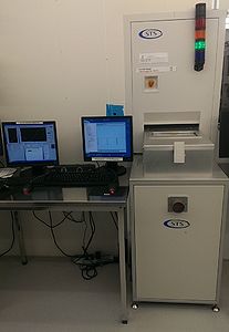
The III-V ICP
Name: PRO ICP
Vendor: STS (now SPTS)
The III-V ICP is a state-of-the-art etch tool. The combination of advanced hardware and software enables you to either use the optimized standard processes or to tailor etch processes for your specific needs. The tool can be used for etching of different materials, but is primarily intented for etching of III-V materials. There are two endpoint systems connected to the system. An Optical End Point System (OES) and a LASER End Point system (LEP). Information on these can be found here: Specific Process Knowledge/Etch/DryEtchProcessing
The user manual, user APV and contact information can be found in LabManager:
Equipment info in LabManager
Process information
Etch recipes
| Purpose | Dry etch of |
| |||||||||
|---|---|---|---|---|---|---|---|---|---|---|---|
| Performance | Etch rates |
| |||||||||
| Anisotropy |
| ||||||||||
| Process parameter range | Process pressure |
| |||||||||
| RF Generators |
| ||||||||||
| Chiller temperature |
| ||||||||||
| Gas flows |
| ||||||||||
| Substrates | Batch size |
| |||||||||
| Substrate material allowed |
| ||||||||||
| Possible masking material |
|
Additional information
Endpoint detection
The III-V ICP is equipped with two endpoint detection systems - an optical endpoint detection system and a laser interferometric system. Click here to access the page common to all dry etch tools that are equipped with an optical endpoint detection system.
Wafer bonding
To find information on how to bond wafers or chips to a carrier wafer, click here.
