LabAdviser: Difference between revisions
No edit summary |
No edit summary |
||
| Line 1: | Line 1: | ||
[[image:Forside20130308 4.jpg|right|500x500px]] | |||
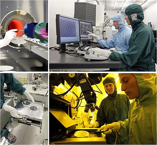
LabAdviser is a process handbook for equipment and processes at the DTU Danchip cleanroom facilities. The function and capacity of each piece of equipment is described in detail and general process steps, eg photolithography procedures, are clarified. LabAdviser is meant to advise you to a good starting point for your cleanroom process for further optimization to meet your needs. To enter LabAdviser you need to '''log in with your DTU login'''. LabAdviser is only editable for Danchip employees. If you need further information about certain machinery or processes, please contact the Danchip personnel. Any feedback you might have on LabAdviser is welcome and can be given by mail to the LabAdviser mailbox: [mailto:labadviser@danchip.dtu.dk labadviser@danchip.dtu.dk] | LabAdviser is a process handbook for equipment and processes at the DTU Danchip cleanroom facilities. The function and capacity of each piece of equipment is described in detail and general process steps, eg photolithography procedures, are clarified. LabAdviser is meant to advise you to a good starting point for your cleanroom process for further optimization to meet your needs. To enter LabAdviser you need to '''log in with your DTU login'''. LabAdviser is only editable for Danchip employees. If you need further information about certain machinery or processes, please contact the Danchip personnel. Any feedback you might have on LabAdviser is welcome and can be given by mail to the LabAdviser mailbox: [mailto:labadviser@danchip.dtu.dk labadviser@danchip.dtu.dk] | ||
<br> | <br> | ||
<br> | <br> | ||
'''News in LabAdviser:''' <br/> | '''News in LabAdviser:''' <br/> | ||
| Line 16: | Line 17: | ||
*'''[[/Process flow approval|Process flow approval]]''' | *'''[[/Process flow approval|Process flow approval]]''' | ||
*'''[[Specific Process Knowledge]]''' | *'''[[Specific Process Knowledge]]''' | ||
*'''[[/Equipment List|Equipment List]]''' | *'''[[/Equipment List|Equipment List]]''' | ||
*'''[[/New equipment in the pipeline and Old equipment for decommissioning|New equipment in the pipeline and old equipment for decommissioning]]''' | *'''[[/New equipment in the pipeline and Old equipment for decommissioning|New equipment in the pipeline and old equipment for decommissioning]]''' | ||
*'''[[Surveys and statistics|Surveys, statistics, monthly LabAdviser updates and other info.]]''' | *'''[[Surveys and statistics|Surveys, statistics, monthly LabAdviser updates and other info.]]''' | ||
*'''[[How to add information to LabAdviser]]''' | *'''[[How to add information to LabAdviser]]''' | ||
---- | <br clear="all" /> | ||
*'''Overview of sample processing: how can you process your sample at DTU Danchip where do you finde the information in LabAdviser''' | |||
{| style="color: black;vertical-align:top" width="100%" border=0 cellpadding="4" cellspacing="0" | |||
| colspan="2" | | |||
|- | |||
| style="width: 50%; vertical-align:top;"| | |||
{| id="linkTable" border="1" cellpadding="0" cellspacing="0" style="text-align:center;" | |||
! class="hideImage" style="display:none"| Front Image | |||
! style="display:none"|- | |||
! style="display:none"|- | |||
! style="display:none"|- | |||
|- | |||
! class="hideImage" width="150" height="180px"| Clean your sample[[file:jehanClean.png|130px|frameless ]] | |||
! class="hideImage" width="150" | Dry your sample [[file:jehanDry.png|130px|frameless ]] | |||
! class="hideImage" width="150" | Create a thin film on your sample [[file:jehanfilm.png|130px|frameless ]] | |||
! class="hideImage" width="150" | Dope your sample [[file:jehanDope.png|130px|frameless ]] | |||
|- | |||
! class="hideImage" width="150" height="180px"| Thermal treatment of your sample [[file:jehanThermal.png|130px|frameless ]] | |||
! class="hideImage" width="150" | Make a mask on your sample[[file:jehanmask.png|130px|frameless ]] | |||
! class="hideImage" width="150" | Transfer pattern to your sample [[file:jehanTransfer.png|130px|frameless ]] | |||
! class="hideImage" width="150" | Define your structure directly [[file:jehandefine.jpg|130px|frameless ]] | |||
|- | |||
! class="hideImage" width="150" height="180px"| Bond your samples together [[file:jehanBond.png|130px|frameless ]] | |||
! class="hideImage" width="150" | Characterize your sample [[file:jehanCharacterize.png|130px|frameless ]] | |||
! class="hideImage" width="150" | Pack your sample [[file:jehanPack.png|130px|frameless ]] | |||
! | | |||
|- | |||
|} | |||
| style="color:black; width: 50%; vertical-align: top;"| | |||
{| class="wikitable hideable hidden" border="1" cellspacing="0" cellpadding="0" align="left" width="430px" style="float:right;" | |||
! style="text-align:right;" | [[|right|500x500px]] | |||
|- | |||
|} | |||
| style="color:black; width: 50%; vertical-align: top"| | |||
{| class="wikitable hideable hidden" border="1" cellspacing="0" cellpadding="0" align="left" width="430px" | |||
! colspan="3" style="text-align:left;" | [[image:Clean your sample.png|x100px|Clean your sample]] Clean your sample | |||
|- | |||
!Entry page in LabAdviser | |||
!Techniques | |||
!Materials | |||
|- | |||
|rowspan="5" valign="top" |[[Specific Process Knowledge/Wafer cleaning|Wafer cleaning]] | |||
|Soap Sonic | |||
|Removes dust and particles | |||
|- | |||
|7-up & Piranha | |||
|Removes traces of organics and alkali ions | |||
|- | |||
|RCA | |||
|Two step process to remove traces of organics and metals | |||
|- | |||
|5% HF | |||
|Removes native oxide | |||
|- | |||
|IMEC | |||
|Removing dust, traces of organics and alkali ions and slightly polish the surface. | |||
Make the surface hydrophillic | |||
|- | |||
|} | |||
{| class="wikitable hideable hidden" border="1" cellspacing="1" cellpadding="2" align="left" width="430px" | |||
!colspan="3" style="text-align:left;" | [[image:Dry your sample.png|x100px|Dry your sample]] Dry your sample | |||
|- | |||
!Entry page in LabAdviser | |||
!Techniques | |||
!Materials | |||
|- | |||
|rowspan="4" valign="top" |[[Specific Process Knowledge/Wafer and sample drying|Wafer and sample drying]] | |||
|Spin dryers | |||
|Whole wafers | |||
|- | |||
|Critial point dryer | |||
|Sensitive wafers | |||
|- | |||
|Ethanol fume drying | |||
|Sensitive wafers | |||
|- | |||
|N2 blow drying | |||
|N2 pistols | |||
|- | |||
|} | |||
{| class="wikitable hideable hidden" border="1" cellspacing="1" cellpadding="2" align="left" width="600px" | |||
!colspan="3" style="text-align:left;" | [[image:Create a film on your sample.png|x100px|Create a layer/film on your sample]] Create a layer/film on your sample | |||
|- | |||
!Entry page in LabAdviser | |||
!Techniques | |||
!Materials | |||
|- | |||
|[[Specific Process Knowledge/Thermal Process/Oxidation| Thermal Process/Oxidation]] | |||
|Thermal oxidation | |||
|Thermal SiO2 | |||
|- | |||
|rowspan="7" valign="top"|[[Specific Process Knowledge/Thin film deposition| Thin film deposition]] | |||
|Sputter deposition | |||
|Metals: Al, Ti, Cr, Co, Ni, Cu, Mo, Pd, Ag, Sn, Ta, W, Pt, Au, Fe, Mg, Nb, Ru <br> | |||
Semiconductors: Si, Ge, ZnO <br> | |||
Oxides: SiO<sub>2</sub>, ITO, TiO<sub>2</sub>, Al<sub>2</sub>O<sub>3</sub>, MgO, Ta<sub>2</sub>O<sub>5</sub> Cr<sub>2</sub>O<sub>3</sub><br> | |||
Transparent Conducting Oxides: ITO, AZO<br> | |||
Alloys: TiW, NiCr, AlTi, NiV, AlCu, CoFe, CuTi, FeMn, MnIr, NiCo, NiFe, YSZ <br> | |||
|- | |||
|Thermal evaporation | |||
|Al, Ge, Ag | |||
|- | |||
|E-beam evaporation | |||
|Metals: Ti, Cr, Al, Ni, Pt, Au, Mo, Pd, Ag, Cu, W, Ta <br> | |||
Semiconductors: Si, Ge <br> | |||
Oxides: SiO<sub>2</sub>, TiO<sub>2</sub> <br> | |||
Alloys: NiCr, TiAl | |||
|- | |||
|LPCVD | |||
|Si<sub>3</sub>N<sub>4</sub>, SRN, SiO<sub>2</sub>, Si (poly and amorph) | |||
|- | |||
|PECVD | |||
|Si<sub>3</sub>N<sub>4</sub>, SiO<sub>2</sub>, PBSG | |||
|- | |||
|Electroplating | |||
|Ni | |||
|- | |||
|Epitaxial growth /MOCVD | |||
|Al, As, Ga, In, P. doping: Si, Zn | |||
|- | |||
|rowspan="2" valign="top"| [[Specific Process Knowledge/Lithography/Coaters|Lithography/Coaters]] | |||
|Spin coating | |||
|resists, polymers | |||
|- | |||
|Spray coating | |||
|resists, polymers | |||
|- | |||
|} | |||
{| class="wikitable hideable hidden" border="1" cellspacing="1" cellpadding="2" align="left" width="430px" | |||
!colspan="3" style="text-align:left;" | [[image:Dope your sample.png|x100px|Dope your sample]] Dope your sample | |||
|- | |||
|- | |||
!Entry page in LabAdviser | |||
!Techniques | |||
!Materials | |||
|- | |||
|rowspan="5" valign="top"| [[Specific Process Knowledge/Doping|Doping]] | |||
|Ion implant | |||
|e.g. P, B, As | |||
|- | |||
|[[Specific Process Knowledge/Thin film deposition/PECVD| PECVD]] | |||
|Deposition of SiO2 or Si3N4 doped with P,B and Ge | |||
|- | |||
|[[Specific Process Knowledge/Thin film deposition/Furnace LPCVD PolySilicon|LPCVD ]] | |||
|Deposition of PolySi doped with B or P | |||
|- | |||
|[[Specific Process Knowledge/Thermal Process/Dope with Boron|Predeposition and drive-in]] | |||
|Doping Silicon wafers with boron | |||
|- | |||
|[[Specific Process Knowledge/Thermal Process/Dope with Phosphorus|Predeposition and drive-in]] | |||
|Doping Silicon wafers with phosphorus | |||
|- | |||
|} | |||
{| class="wikitable hideable hidden" border="1" cellspacing="1" cellpadding="2" align="left" width="430px" | |||
!colspan="3" style="text-align:left;" | [[image:Thermal treat your sample.png|x100px|Thermal treatment of your sample]] Thermal treatment of your sample | |||
|- | |||
!Entry page in LabAdviser | |||
!Techniques | |||
!Materials | |||
|- | |||
|rowspan="5" valign="top"|[[Specific Process Knowledge/Thermal Process|Thermal Process]] | |||
|Annealing (>350C) | |||
|Si, PECVD layers, Al, BCB curing, Polymer | |||
|- | |||
|Oxidation | |||
|Si wafers | |||
|- | |||
|Doping with B/P | |||
|Si wafers | |||
|- | |||
|Pyrolysis | |||
|Resists: AZ, SU8, PDMS | |||
|- | |||
|Rapid Thermal Anneal (RTP) | |||
|SiO2, Si3N4, Ti, III-V | |||
|- | |||
| | |||
[[Specific Process Knowledge/Lithography/Baking| Lithography/Baking]] <br> | |||
|Baking (<300dg) | |||
|baking resist and polymers | |||
|- | |||
|} | |||
{| class="wikitable hideable hidden" border="1" cellspacing="1" cellpadding="2" align="left" width="430px" | |||
!colspan="3" style="text-align:left;" | [[image:Make a mask on your sample.png|x100px|Make a mask on your sample]] Make a mask on your sample | |||
|- | |||
!Entry page in LabAdviser | |||
!Techniques | |||
!Materials | |||
|- | |||
|rowspan="5" valign="top"|[[Specific Process Knowledge/Lithography| Lithography]] | |||
|Pattern design | |||
| | |||
|- | |||
|Photolithography | |||
|UV resists | |||
|- | |||
|Deep UV lithography | |||
|DUV resists | |||
|- | |||
|E-beam lithography | |||
|E-beam resists | |||
|- | |||
|Imprinting | |||
|Polymers | |||
|- | |||
|} | |||
{| class="wikitable hideable hidden" border="1" cellspacing="1" cellpadding="2" align="left" width="430px" | |||
!colspan="3" style="text-align:left;" | [[image:Transfer mask pattrn to your sample.png|x100px|Transfer mask pattern to your sample]] Transfer mask pattern to your sample | |||
|- | |||
!Entry page in LabAdviser | |||
!Techniques | |||
!Materials | |||
|- | |||
|rowspan="2" valign="top"|[[Specific Process Knowledge/Etch| Etch]] | |||
|Wet etch | |||
|Si, Glass, SiO2, Si3N4, Al, Cr, Ti, Au, Pt, InP, InGaAsP, GaAs/AlGaAs | |||
|- | |||
|Dry etch | |||
|Any material | |||
|- | |||
|[[Specific Process Knowledge/Lithography/LiftOff| Lithography/Lift-off]] | |||
|Lift-off | |||
|Most materials | |||
|- | |||
|} | |||
{| class="wikitable hideable hidden" border="1" cellspacing="1" cellpadding="2" align="left" width="430px" | |||
!colspan="3" style="text-align:left;" | [[image:Define your structure directly.png|x100px|Define the structure directly on your sample]] Define your structure directly | |||
|- | |||
!Entry page in LabAdviser | |||
!Techniques | |||
!Materials | |||
|- | |||
|rowspan="5" valign="top"|[[Specific Process Knowledge/Direct Structure Definition|Direct Structure Definition]] | |||
|Polymer Injection molding | |||
|Topas, PP, PE, PS | |||
|- | |||
|LASER micro machining | |||
|Silicon, Metal, Graphene (on silicon), Glass (Pyrex, fused silica), TOPAS, PMMA | |||
|- | |||
|Dicing saw | |||
|Silicon, Glass (Pyrex, fused silica) | |||
|- | |||
|[[Specific Process Knowledge/Imprinting|Imprinting]] | |||
|TOPAS, PMMA | |||
|- | |||
|[[Specific Process Knowledge/Lithography|Lithography definition]] | |||
|SU8, AZ resists | |||
|- | |||
|} | |||
{| class="wikitable hideable hidden" border="1" cellspacing="1" cellpadding="2" align="left" width="430px" | |||
!colspan="3" style="text-align:left;" | [[image:Bond your samples together.png|x100px|Bond your samples together]] Bond your samples together | |||
|- | |||
!Entry page in LabAdviser | |||
!Techniques | |||
|- | |||
|rowspan="3" valign="top"|[[Specific Process Knowledge/Bonding|Bonding]] | |||
|Eutectic bonding | |||
|- | |||
|Fusion bonding | |||
|- | |||
|Anodic bonding | |||
|- | |||
|[[Specific_Process_Knowledge/Etch/DryEtchProcessing/Bonding |Etch/DryEtchProcessing/Bonding]] | |||
|Temporary bonding of wafers or chips for dry etching | |||
|- | |||
|} | |||
{| class="wikitable hideable hidden" border="1" cellspacing="1" cellpadding="2" align="left" width="430px" | |||
!colspan="3" style="text-align:left;" | [[image:Characterize your sample.png|x100px|Characterize your sample]] Characterize your sample | |||
|- | |||
!Entry page in LabAdviser | |||
!What do you need to measure? | |||
!Technique/Method | |||
|- | |||
|rowspan="12" valign="top"|[[Specific Process Knowledge/Characterization|Characterization]] | |||
|Sample Imaging, XY dimensions | |||
|Microscopy: optical, SEM, AFM | |||
|- | |||
|Sample Topography | |||
|AFM, Profiling with stylus or optical | |||
|- | |||
|Film thickness and optical constants | |||
|Ellipsometry, Reflectometry, Prism Coupling | |||
|- | |||
|Film Stress | |||
|Profiling with stylus or optical | |||
|- | |||
|Wafer thickness | |||
|Micrometer gauge | |||
|- | |||
|Element analysis | |||
|XPS, EDX, SIMS | |||
|- | |||
|Contact Angle | |||
|Drop shape analyzing | |||
|- | |||
|Resistivity | |||
|Four point probe, Probe station | |||
|- | |||
|Doping level/Carrier density | |||
|ECV (Electrochemical Capacitance-Voltage) -profiler | |||
|- | |||
|Direct Bandgap | |||
|Photoluminescence | |||
|- | |||
|Lattice mismatch | |||
|X-ray diffractometer | |||
|- | |||
|Defects/contamination | |||
|Particle/defect counter | |||
|- | |||
|} | |||
{| class="wikitable hideable hidden" border="1" cellspacing="1" cellpadding="2" align="left" width="430px" | |||
!colspan="3" style="text-align:left;" | [[image:Pack your sample (back-end).png|x100px|Pack your sample (back-end)]] Pack your sample (back-end) | |||
|- | |||
!Entry page in LabAdviser | |||
!Techniques | |||
|- | |||
|rowspan="3" valign="top"|[[Specific Process Knowledge/Back-end processing|Back-end processing]] | |||
|Chip/die mounting | |||
|- | |||
|Wire bonding | |||
|- | |||
|Dicing | |||
|- | |||
|} | |||
| | |||
|- | |||
|} | |||
Revision as of 14:49, 18 December 2014
LabAdviser is a process handbook for equipment and processes at the DTU Danchip cleanroom facilities. The function and capacity of each piece of equipment is described in detail and general process steps, eg photolithography procedures, are clarified. LabAdviser is meant to advise you to a good starting point for your cleanroom process for further optimization to meet your needs. To enter LabAdviser you need to log in with your DTU login. LabAdviser is only editable for Danchip employees. If you need further information about certain machinery or processes, please contact the Danchip personnel. Any feedback you might have on LabAdviser is welcome and can be given by mail to the LabAdviser mailbox: labadviser@danchip.dtu.dk
News in LabAdviser:
The latest monthly LabAdviser update: LabAdviser update send out 2014-11-25
Slides from the customer meeting December 2013: Customer meeting 2013
Contents
- Danchip contact information
- Introduction to LabAdviser and Processing
- Introduction to LabManager
- Process flow approval
- Specific Process Knowledge
- Equipment List
- New equipment in the pipeline and old equipment for decommissioning
- Surveys, statistics, monthly LabAdviser updates and other info.
- How to add information to LabAdviser
- Overview of sample processing: how can you process your sample at DTU Danchip where do you finde the information in LabAdviser
Danchip Contact Info
In order to get the quickest response to training requests, process approvals, questions etc. please use the following mailboxes to DTU Nanolab (formerly known as Danchip).
| Subject | Description | |
| Training and Process Flow | training@nanolab.dtu.dk | All requests regarding equipment training and process flows. Please add your Name to the subject line. Note: Requests are commonly answered within 2 workdays. |
| E-beam training | e-beam@nanolab.dtu.dk | Requests regarding training on JEOL JBX-9500FSZ or Raith Eline e-beam systems. Please study the material on the EBL Labadviser pages beforehand. |
| E-beam Cassette loading | e-beamload@nanolab.dtu.dk | Requests regarding cassette loading on JEOL JBX-9500FSZ. |
| General inquiries | nanolabsupport@nanolab.dtu.dk | Inquiries related to machines, cleanroom access, Mask review, tool changes, and others. Please add your Name to the subject line. Note: Requests are commonly answered within 2 workdays. |
| Metal Wishes | metal@nanolab.dtu.dk | Requests for change of metal in Thin Film Deposition equipment. See current and future materials in statuslog of the respective machines.
|
| Gas-related Requests | DCH-Gas@nanolab.dtu.dk | All topics gas-related (issues, information regarding ordering, delivery, changing etc). Mostly for internal DTU Nanolab use. |
| LabAdviser Mailbox | labadviser@nanolab.dtu.dk | Any questions or feedback to LabAdviser. |
| Commercial Inquiries | sales@nanolab.dtu.dk | For all inquiries regarding in-sourcing, commercial applications, rent of cleanroom space, etc |
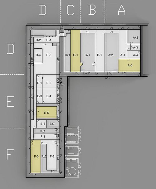
Cleanroom naming and phone numbers
|
|
| |||||||||||||||||||||||||||||||||||||||||||||||||||
