Specific Process Knowledge/Thermal Process/Dope with Phosphorus
Feedback to this page: click here
The Phosphorus Predep furnace (A4) can be used for phosphorus pre-deposition of silicon wafers, resulting in n-type doping. In the furnace, the silicon wafers are positioned vertically in a quarts boat.
Test of the Phosphorus Predep furnace
This page is written by DTU Nanolab internal
Purpose
To study the correlation between the temperature for the predeposition process and drive-in of the phosphorus doping in the Phosphorus Predep furnace (A4) at DTU Nanolab.
Experimental setup
20 boron doped device wafers (p-type) were used - Four wafers for each of the five different predeposition temperatures (see table below). In the furnace five dummy wafers were placed on each side of the device wafers. The dummy wafers nearest to the device wafers were changed in-between the runs to minimize doping from these dummy wafers.
| Run # | Temperature | Process time with POCl3 | Annealing time in O2 | Wafer # |
|---|---|---|---|---|
| 1 | 850 oC | 15 minutes | 20 minutes | 1, 2, 3, 4 |
| 2 | 900 oC | 15 minutes | 20 minutes | 5, 6, 7, 8 |
| 3 | 950 oC | 15 minutes | 20 minutes | 9, 10, 11, 12 |
| 4 | 1000 oC | 15 minutes | 20 minuntes | 13, 14, 15, 16 |
| 5 | 1050 oC | 15 minutes | 20 minutes | 17, 18, 19, 20 |
After the predeposition two wafers from each run were taken out to be further processed. These wafers were: 1, 2, 5, 6, 9, 10, 13, 14, 17, 18. These wafers were dipped in BHF to remove the phosphorus glass layer before the drive-in process.
The drive-in process was made in the Phosphorus Drive-in furnace (A3) for all the mentioned wafers at same time. At the drive-in process a dummy wafer was placed in-between the wafers that have been predeposited at different temperatures, so doping from wafer to wafer was minimized. The phosphorus drive-in was done with the process "DRY1050" which is a dry oxidation at 1050 oC for 100 minutes and 20 minutes annealing. At the oxidation the O2 flow was 5 SLM, and the N2 flow for annealing was 3 SLM.
Results
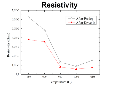
Several measurements were done for the different device wafers. After the predeposition, the thickness of the grown phosphorus glass layer was measured, and the sheet resistance and slice resistivity were measured on the same wafer after a BHF etch.
| Ellipsometer (center point only) | Four Point Probe | ||||
|---|---|---|---|---|---|
| Wafer # | Temperature [C] | Oxide thickness [nm] | Refractive index | Sheet resistance [Ωsq] | Slice Resistivity [Ωcm] |
| 3 | 850 | 27,4 | 1,4623 | 311 | 6,22*10-3 |
| 7 | 900 | 45,27 | 1,4622 | 138,5 | 4,85*10-3 |
| 11 | 950 | 61,36 | 1,4625 | 16,1 | 1,29*10-3 |
| 15 | 1000 | 80,45 | 1,4624 | 7,4 | 0,89*10-3 |
| 19 | 1050 | 119,37 | 1,4623 | 6,6 | 1,49*10-3 |
The oxide layer was etch in BHF before the drive-in of the doping with a dry oxidation at 1050 oC for 100 minutes and 20 minutes annealing.
| Avg. five point on Filmtek | Four Point Probe | ||||
|---|---|---|---|---|---|
| Wafer # | Temperature [oC] | Oxide thickness [nm] | Refractive index | Sheet resistance [Ωsq] | Slice Resistivity [Ωcm] |
| 2 | 850 | 110,44 | 1,4654 | 189,7 | 3,79*10-3 |
| 6 | 900 | 116,28 | 1,4629 | 101,6 | 3,56*10-3 |
| 9 | 950 | 137,06 | 1,4604 | 10,0 | 0,8*10-3 |
| 14 | 1000 | 141,46 | 1,4651 | 4,72 | 0,57*10-3 |
| 18 | 1050 | 139,87 | 1,4659 | 3,23 | 0,73*10-3 |
| Blank Si wafer | 110,71 | 1,46286 | - | - | |
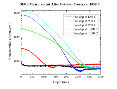
Looking at the "SIMS Measurement After Drive-in Process at 1050 oC" graph, it can be seen that the two curves "Pre-dep at 950 oC" and "Pre-dep at 1000 oC" are crossing each other, but according to the theory they should not do that. Only one wafer has been measured so there is not that much statistical data to verify it with.
Test of the Phosphorus Predep furnace
This page is written by DTU Nanolab internal
Purpose
To find the result of a specific process using the Phosphorus Predep furnace (A4) followed by a drive in and oxidating the substrate in the Phosphorus drive in furnace (A3).
Experimental setup
Substrate: p-type Si(100,)
Resistivity: 1-20 Ωcm
Recipe: POCL900
Temperature: 900 °C
Time: 15 min
Anneal: 20 min in N2
After removing the oxide in BHF the wafers were oxidized in Phosphor Drive in Furnace (A3) using DRY1050 at 1050°C for 70 min without further annealing in N2. Results are listed in the table below:
Results
| Afer predeposition | After Oxidation | ||
|---|---|---|---|
| Test date | Sheet resistance [Ω/sq] | Oxide thickness [nm] | Sheet resistance [Ω/sq |
| Aug2012 | 47.0 | 93.1 | 41.8 |
| Jan2013 | 50.5 | 91.3 | 55.6 |
| Aug2013 | 58.0 | 91.8 | 41.8 |
| Jan2014 | 54.1 | 93.3 | 33.8 |
| Jan2015 | 50.8 | 94.2 | 39.4 |
One wafer from Jan2015 was analyzed with SIMS and the profile is shown on the graph below:
Result from GreenBelt, @nanolab,Jan 2015
Test of the Phosphorus Predep furnace
Purpose
To find the doping profile after a specific process flow. The test was made by only performing the high-temperature process step after the pre-deposition step done in the Phosphorus Predep furnace (A4). The subsequently high temperature processes was done by using the Phosphorous drive in furnace (A3) and the Oxide Anneal Furnace (C3).
Experimental setup
Substrate: p-type Si(100,)
Resistivity: 1-20 Ωcm
The total thermal budget for the wafers:
Predeposition in Furnace (A4): POCL1000, 15 min, no further anneal
Wet Oxidation in Furnace (A3): WET1050, 30 min, no further anneal
Anneal in Furnace (C1): ANN1000, 30 min in N2
Wet oxidation in Furnace (C1): WET1050, 30 min, no further anneal
Results
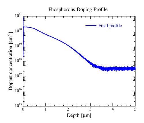
The wafer was analyzed with SIMS and the profile is shown on the graph below:
Result from Trine Holm Christensen, @Space, Feb. 2015
Phosphorous doping test after hardware and software upgrades
This page is written by DTU Nanolab internal
In 2022, the POCl3 line on the furnace was modified to make the setup more safe. At the same time some software changes were also made, and the recipes on the furnace were updated.
Afterwards, a phosphorus doping test was made to see, if the modification had affected the phosphorus doping process. The test was done with a test wafer and four dummy wafers (two dummy wafers on each side of the test wafers) in the furnace.
Process:
- RCA cleaning of the test wafer (p-type, 1-20 Ωcm) and the dummy wafers
- Phosphorus pre-deposition in the Phosphorus Pre-dep furnace (A4).
- Recipe: "POCL900"
- Temperature: 900 °C
- Time: 15 min phosphorus pre-dep and 20 min annealing/N2 post purge
- BHF dip in the RCA cleaning bench to remove phosphorus glass from the test wafer
- Measure sheet resistance using the 4-point proble
Results:
After the process describe above, the sheet resistance on the test wafer was measured.
The sheet resistance was 54 Ωsq in the center of the wafer and 45-48 Ωsq in the edge of the wafer. This correspond quite good to the results that previously had been obtained for the furnace as can be seen on this LabAdviser page.
Notes about the POCL recipes
A new recipe for POCL doping called was made, after the POCl3 line was modified. The N2 high flow (3 SLM) is on all the time through the recipe. There is a 2 min pre-purge with first N2 low (150 sccm) through the POCl3 bubbler, i.e. with the valves v4a and v4b closed, and then with O2 (0.50 SLM), before the pre-deposition time starts. After the pre-deposition, an N2 low post-purge (500 sccm) is done for 2 minutes with v4a and v4b closed.
For safety reasons it is important that the POCl3 is completely removed from the furnace, before it is opened to load or unload wafers.
With 150 sccm N2 low through 25°C POCl3 liquid + 3 slm N2 high + 0.5 slm O2, 3300 ppm Cl2 is created in the tube. These 3300 ppm Cl2 must be diluted to less than 0.5 ppm (the TLV value).
The tube diameter is 16 cm and the length without ball valve is about 125 cm, and thus the volume is about 25 L. After the phosphorus pre-deposition step, the N2 high flow (3 SLM) is on during the annealing/N2 post purge, the cooling and a waiting step. The time for the waiting step is 30 minutes, so even if the annealing time is set to 0 minutes, and the furnace does not have to cool down, there will still be an N2 high flow for 30 minutes to remove the POCl3 from the furnace. The waiting time is the same in the abort recipe that is activated, if the POCL doping recipe is aborted.
The recipe can be modified with other temperatures and names.


