Specific Process Knowledge/Thin film deposition/Wordentec
Feedback to this page: click here
Unless otherwise stated, this page is written by DTU Nanolab internal
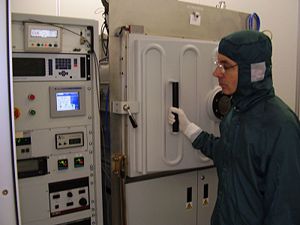
Wordentec QCL 800
The Wordentec is a machine for:
- Deposition of metals by e-beam evaporation
- Deposition of metals by thermal evaporation
- Deposition of materials by DC sputtering
- Cleaning samples before deposition by Argon RF sputter cleaning
The Wordentec is designed to deposit on 1-6 samples in sequence. Adaptors exist for deposition on 2", 4" and 6" wafers and deposition is possible on samples of almost any size and shape, as long as they do not exceed a 6" diameter. The Wordentec supports either single sample deposition for running a separate recipe on each sample or batch deposition for six wafers in sequence. It is possible to freely combine processes from the machine's different sources.
The user manual, quality control procedure and results, user APV, technical information and contact information can be found in LabManager:
Process information
The metals available for E-beam evaporation and their standard deposition rates are:
| Metal | Deposition rate [Å/s] |
|---|---|
| Titanium (Ti) | 10 |
| Chromium (Cr) | 10 |
| Aluminium (Al) | 10 |
| Nickel (Ni) | 10 |
| Platinum (Pt) | 10 |
| Gold (Au) | 10 |
Temperature and roughness studies of Au deposition processes in the Wordentec
E-beam evaporation of some materials like Au and Al can affect the underlying layers and thin resists such as E-beam sensitive resists can get exposed or their topography may change. Cases of releasing bubbles of the solvent will create a crater-like surface on some materials. In most cases this only affects the areas containing resist, hence liftoff is often easier and the areas without resist will have good adhesion.
Delaminating Au film on thin E-beam resist
Thermal evaporation materials
We currently have Aluminium, Silver and Germanium available to deposit through thermal evaporation.
Sputter materials
It is possible to sputter deposit almost any material, provided that it is possible to deposit with DC sputtering. The materials available currently include:
- TiW alloy (10%/90% by weight)
- Aluminium (Al)
- Chromium (Cr)
- Silver (Ag)
- Titanium (Ti)
- Silicon (Si)
- NiV alloy
More information about deposition rates and surface roughness can be found by clicking on the different elements.
Thickness measurement
Read about how the machine measures the thickness of the growing film using a quartz crystal monitor here.
Particulates in the films
Read about some tests that we made of particulates in e-beam evaporated Al, Ni, and TiAu films made in the Wordentec and the Temescal here.
| Purpose | Deposition of metals |
|
|---|---|---|
| Performance | Film thickness |
|
| Deposition rate |
| |
| Thickness uniformity |
| |
| Process parameter range | Process Temperature |
|
| Process pressure |
| |
| Substrates | Batch size |
|
| Substrate material allowed |
| |
| Material allowed on the substrate |
|
* For e-beam evaporation and sputtering, permission is required for thicknesses above 600 nm. For thermal evaporation, permission is required for thicknesses above 120 nm. This is to ensure that there will be enough material present. Contact metal@nanolab.dtu.dk or thinfilm@nanolab.dtu.dk
** Percent variation calculated as (Max-Min)/Average. For thermally evaporated Al, the max was on one side of the wafer rather than in the middle. Measured by Rebecca Ettlinger, Nov. 2018.
