Specific Process Knowledge/Thin film deposition/Deposition of Silicon Nitride/Deposition of Silicon Nitride using PECVD/PECVD3: Low stress nitride testing
< Specific Process Knowledge | Thin film deposition | Deposition of Silicon Nitride | Deposition of Silicon Nitride using PECVD
Jump to navigation
Jump to search
Feedback to this page: click here
Unless otherwise stated, this page is written by DTU Nanolab internal
Stress variation with LF/HF timing (Thomas Pedersen @ DTU Nanolab 2018)
In late 2018 a series of experiments trying to control the stress level in silicon nitride deposited on PECVD3 were made. The only parameter changed was the timing between the high frequency and low frequency periods. Experiments were made on 690 µm thick 6" wafers, no quartz carrier was used. Default parameters of the mfsinls2 recipe are listed below.
| SiH4 [sccm] | NH3 [sccm] | N2 [sccm] | Pressure [mTorr] | HF Time [s] | HF Power [W] | HF Load [%] | HF Tune [%] | LF Time [s] | LF Power [W] | LF Load [%] | LF Tune [%] |
|---|---|---|---|---|---|---|---|---|---|---|---|
| 30 | 30 | 1470 | 845 | 7.8 | 100 | 70 | 68 | 2.2 | 100 | 5.4 | 48.8 |
Timing changes and measured stress are listed below.
| Date | Time [mm:ss] | HF Time [s] | LF Time [s] | Thickness [nm] | Std.Dev [nm] | Rate [nm/min] | RI [] | Stress [Mpa] | |
|---|---|---|---|---|---|---|---|---|---|
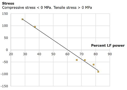
| 20-08-2018 | 23:00 | 7.8 | 2.2 | 1143 | 23 | 48.1 | 2.040 | 127 | Tensile |
| 24-08-2018 | 23:00 | 7.3 | 2.7 | 1184 | 15 | 51.5 | 2.040 | 96 | Tensile |
| 04-09-2018 | 22:00 | 6.0 | 4.0 | 1190 | 13 | 54.1 | 2.000 | 41.5 | Compressive |
| 04-09-2018 | 18:30 | 5.8 | 4.2 | 1007 | 9 | 54.4 | 2.010 | 42.2 | Compressive |
| 11-09-2018 | 18:30 | 5.5 | 4.5 | 1026 | 9 | 55.5 | 2.001 | 90 | Compressive |
| 22-10-2018 | 18:30 | 11.2 | 8.8 | 1008 | 6.2 | 54.5 | 2.011 | 61 | Compressive |
The stress as function of percent LF power is plotted in the graph below.
DOE made to find a good QC nitride recipe with low stress and low KOH etch rate (by Berit Herstrøm @ DTU Nanolab 2016 Marts)

Analysis of KOH etch rate dependency of process parameters
Analysis of film stress dependency of process parameters
