Specific Process Knowledge/Thin film deposition/Deposition of Silicon Nitride/Deposition of Silicon Nitride using PECVD/MF SiN results
Feedback to this page: click here
MF SiN results from PECVD4
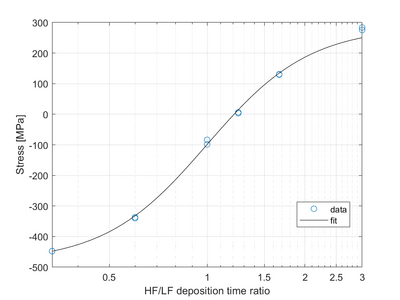
Film stress as a function of the ratio between the high frequency time to the low frequency time in a mixed frequency recipe
The work was made by Dennis Høj @fysik.dtu.dk i November/December 2019

The curve shows the stress as a funktion of x = t_HF/t_LF, t is the deposition time for HF og LF. The cycle time is 8 seconds.
The equation for the fitted line is:
where sigma_HF = 286 MPa and sigma_LF = -484 MPa. Ideally one would expect n = 1 which means that sigma would be the average of the two separate layers. The single layers are expected to be below 1 nm and therefor the layers are probably not well defined seperate layers. The fitting with n = 1 was not good. For the fitted line n = 2.75.
Dennis has made a recipe: Fysik/denho/MFSiN LS with the stress level below 10 MPa, please copy it if you want to use it..
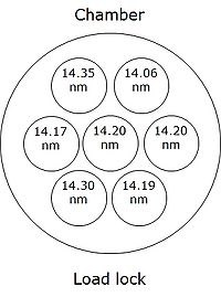
Uniformity results using the carrier 7 times 2" wafers
Experiment was made by Jesper Fly Hansen @ NILT in June 2018
The recipe Mf_SiN was run for 1min 10sec. This gave the following thicknesses on the 7 2" wafers on the carrier made for 7 2" wafers.

