Specific Process Knowledge/Thin film deposition/PECVD: Difference between revisions
No edit summary |
|||
| (2 intermediate revisions by the same user not shown) | |||
| Line 1: | Line 1: | ||
'''Feedback to this page''': '''[mailto:labadviser@nanolab.dtu.dk?Subject=Feed%20back%20from%20page%20http://labadviser.nanolab.dtu.dk/index.php/Specific_Process_Knowledge/Thin_film_deposition/PECVD click here]''' | '''Feedback to this page''': '''[mailto:labadviser@nanolab.dtu.dk?Subject=Feed%20back%20from%20page%20http://labadviser.nanolab.dtu.dk/index.php/Specific_Process_Knowledge/Thin_film_deposition/PECVD click here]''' <br> | ||
[[Category: Equipment|Thin film PECVD]] | [[Category: Equipment|Thin film PECVD]] | ||
[[Category: Thin Film Deposition|PECVD]] | [[Category: Thin Film Deposition|PECVD]] | ||
{{CC1}} | |||
==PECVD Plasma Enhanced Chemical Vapor Deposition== | ==PECVD Plasma Enhanced Chemical Vapor Deposition== | ||
Name PECVD4: PRO CVD <br> | Name PECVD4: PRO CVD <br> | ||
Vendor: SPTS <br> | Vendor: SPTS <br> | ||
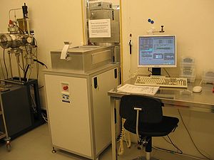
[[image:PECVD3a.jpg|300x300px|right|thumb|PECVD3 - positioned in cleanroom A-1]] | [[image:PECVD3a.jpg|300x300px|right|thumb|PECVD3 - positioned in cleanroom A-1, photo: DTU Nanolab internal]] | ||
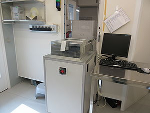
[[image:PECVD4.JPG|300x300px|right|thumb|PECVD4 - positioned in cleanroom B-1]] | [[image:PECVD4.JPG|300x300px|right|thumb|PECVD4 - positioned in cleanroom B-1, photo: DTU Nanolab internal]] | ||
We have two PECVD's here at DTU Nanolab. They can both be used to deposit Silicon oxides and Silicon nitrides with or without dopants of Boron and Phosphorus. PECVD3 can also deposit thin layer of aSi. PECVD3 is used for silicon based processing with small amounts (<5% wafer coverage, under some condition even more) of metals where as PECVD4 is dedicated for clean wafers both for silicon based materials and III-V materials. Quartz carriers are used in PECVD4 and they are dedicated the two different material groups to avoid cross contamination. See the precise rules in the equipment manuals which are uploaded in LabManager. | We have two PECVD's here at DTU Nanolab. They can both be used to deposit Silicon oxides and Silicon nitrides with or without dopants of Boron and Phosphorus. PECVD3 can also deposit thin layer of aSi. PECVD3 is used for silicon based processing with small amounts (<5% wafer coverage, under some condition even more) of metals where as PECVD4 is dedicated for clean wafers both for silicon based materials and III-V materials. Quartz carriers are used in PECVD4 and they are dedicated the two different material groups to avoid cross contamination. See the precise rules in the equipment manuals which are uploaded in LabManager. | ||
| Line 105: | Line 105: | ||
|style="background:LightGrey; color:black"|Gas flows | |style="background:LightGrey; color:black"|Gas flows | ||
|style="background:WhiteSmoke; color:black"| | |style="background:WhiteSmoke; color:black"| | ||
*SiH<sub>4</sub>:0- | *SiH<sub>4</sub>:0-180 sccm | ||
*N<sub>2</sub>O:0-3000 sccm | *N<sub>2</sub>O:0-3000 sccm | ||
*NH<sub>3</sub>:0-1000 sccm | *NH<sub>3</sub>:0-1000 sccm | ||
Latest revision as of 08:53, 26 May 2023
Feedback to this page: click here
Unless otherwise stated, this page is written by DTU Nanolab internal
PECVD Plasma Enhanced Chemical Vapor Deposition
Name PECVD4: PRO CVD
Vendor: SPTS


We have two PECVD's here at DTU Nanolab. They can both be used to deposit Silicon oxides and Silicon nitrides with or without dopants of Boron and Phosphorus. PECVD3 can also deposit thin layer of aSi. PECVD3 is used for silicon based processing with small amounts (<5% wafer coverage, under some condition even more) of metals where as PECVD4 is dedicated for clean wafers both for silicon based materials and III-V materials. Quartz carriers are used in PECVD4 and they are dedicated the two different material groups to avoid cross contamination. See the precise rules in the equipment manuals which are uploaded in LabManager.
PECVD is a chemical vapor deposition process that applies a plasma to enhance chemical reaction rates of reactive species. PECVD processing allows deposition at lower temperatures, which is often critical in the manufacture of semiconductors. PECVD films are however known for not being stochiometeric and normally a lot of hydrogen is incorporated inside the films.
All though PECVD4 and 3 are very similar you should not expect to transfer a recipe between the systems and get the exact same result.
The user manuals, quality control procedures and results, user APVs, technical information and contact information can be found in LabManager (requires login):
PECVD3 in LabManager
PECVD4 in LabManager
Process information on PECVD3 and PECVD4
- Recipes for deposition of silicon oxides
- Recipes on for deposition of silicon nitride and silicon oxynitride
- Doping with boron
- Pre-release tests on PECVD4
| PECVD | PECVD3 | PECVD4 | |
|---|---|---|---|
| Purpose | Deposition of dielectrica |
|
|
| Performance | Film thickness |
|
|
| Index of refraction |
|
| |
| Step coverage |
|
| |
| Film quality |
|
| |
| Process parameter range | Process Temperature |
|
|
| Process pressure |
|
| |
| Gas flows |
|
| |
| Substrates | Batch size |
|
|
| Materials allowed |
|
| |
