Specific Process Knowledge/Thin film deposition/Furnace LPCVD PolySilicon/Boron doped poly-Si and a-Si
Feedback to this page: click here
Unless otherwise stated, this page is written by DTU Nanolab internal
Boron-doped amorphous silicon by using 4" LPCVD polysilicon furnace (B4)
Result from Thomas Pedersen, DTU Nanotech (now DTU Nanolab), September 2015
Process parameters
Pressure: 250 mtorr
Temperature: 580 °C
Silane (SiH4) flow: Constant at 80 sccm
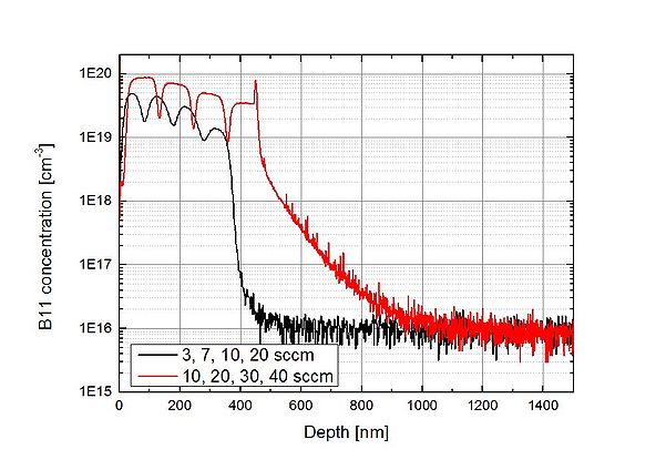
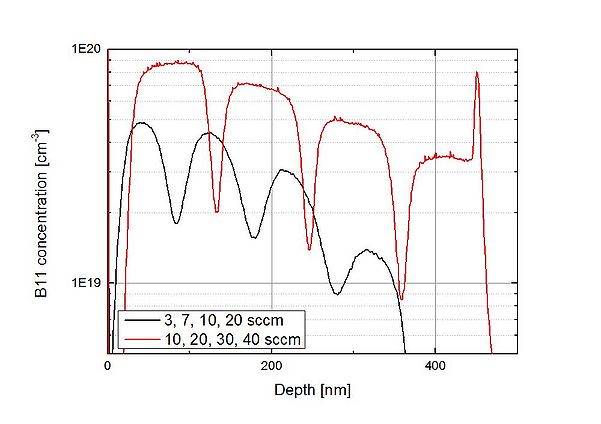
Diborane (B2H6) flow: Varied from 3 sccm to 40 sccm
Anneal: No annealing afterwards
Test wafer position: Center of the boat
Results
The Boron concentration of the film was controlled by the flow of B2H6 gas. To establish how boron doping concentration varied with B2H6 flow, films of silicon were deposited with B2H6 gas flows modulated during deposition to produce doping spikes. The two figures below show a typical SIMS concentration depth profile of a B2H6 modulation-doped film deposited on a Silicon dioxide substrate. During deposition, the gas flow of SiH4 was held constant, while flows of B2H6 was varied to create the dopant spikes.
Boron-doped amorphous silicon by using 4" LPCVD polysilicon furnace (B4)
Result from Trine Holm Christensen, @Space, Feb. 2015
Process parameters
The test was made on a n-type silicon wafer (100) with a 110 nm grown thermal oxide)
Pressure: 250 mtorr
Temperature: 580 °C
Silane (SiH4) flow: 80 sccm
Diborane (B2H6) flow: 7 sccm
Time: 75 min
Anneal: @950°C for 60 min in N2
Test wafer position: Center of the boat
A better uniformity of the resistivity across the wafer was achieved by subsequently annealing in N2, the annealing was done in Anneal Oxide Furnace (C1). The measured film thickness was 370 nm and the sheet resistance was measured to 200 Ω/sq +/- 15 Ω/sq.

