Specific Process Knowledge/Thermal Process/Dope with Phosphorus: Difference between revisions
| Line 93: | Line 93: | ||
|} | |} | ||
The oxide layer was etch in BHF before the drive-in of the doping at 1050 <sup>o</sup>C for 100 minutes and 20 minutes annealing. | |||
{| border="2" cellpadding="2" cellspacing="1" style="text-align:center;" | {| border="2" cellpadding="2" cellspacing="1" style="text-align:center;" | ||
Revision as of 12:40, 21 October 2013
Feedback to this page: click here
The Phosphorus Predep furnace (A4) can be used for phosphorus predeposition of silicon wafers, resulting in N-type doping. In the furnace, the silicon wafers are positioned vertically in a quarts boat.
Test of the Phosphorus Predep furnace
Purpose
To study the correlation between the temperature for the predeposition process and drive-in of the phosphorus doping in the Phosphorus Predep furnace (A4) at DTU Danchip.
Experimental setup
20 boron doped device wafers (p-type) were used - Four wafers for each of the five different predeposition temperatures (see table below). In the furnace five dummy wafers were placed on each side of the device wafers. The dummy wafers nearest to the device wafers were changed in-between the runs to miniminze doping from these dummy wafers.
| Run # | Temperature | Process time with POCl3 | Annealing time in N2 | Wafer # |
|---|---|---|---|---|
| 1 | 850 oC | 15 minutes | 20 miuntes | 1, 2, 3, 4 |
| 2 | 900 oC | 15 minutes | 20 miuntes | 5, 6, 7, 8 |
| 3 | 950 oC | 15 minutes | 20 miuntes | 9, 10, 11, 12 |
| 4 | 1000 oC | 15 minutes | 20 miuntes | 13, 14, 15, 16 |
| 5 | 1050 oC | 15 minutes | 20 miuntes | 17, 18, 19, 20 |
After the predeposition two wafers from each run were taken out to be further processed. These wafers were: 1, 2, 5, 6, 9, 10, 13, 14, 17, 18. These wafers were dipped in BHF to remove the phosphorus glass layer before the drive-in process.
The drive-in process was made in the Phosphorus Drive-in furnace (A3) for all the mentioned wafers at same time. At the drive-in process a dummy wafer was placed in-between the wafers that have been predeposited at different temperatures, so doping from wafer to wafer was minimized. The phosphorus drive-in was done with the process "DRY1050" which is a dry oxidation at 1050 oC for 100 minutes and 20 minutes annealing. At the oxidation the O2 flow was 5 SLM, and the N2 flow for annealing was 3 SLM.
Results
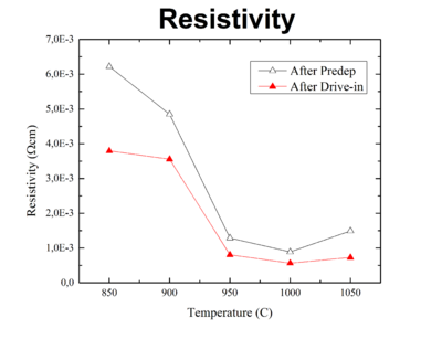
Several measurements were done for the different device wafers. After the predeposition, the thickness of the grown phosphorus glass layer was measured, and the sheet resistance and slice resistivity were measured on the same wafer after a BHF etch.
| Ellipsometer (center point only) | Four Point Probe | ||||
|---|---|---|---|---|---|
| Wafer # | Temperature [C] | Oxide thickness [nm] | Refrative index | Sheet resistance [Ωsq] | Slice Resistivity [Ωcm] |
| 3 | 850 | 27,4 | 1,4623 | 311 | 17,32 |
| 7 | 900 | 45,27 | 1,4622 | 138,5 | 7,61 |
| 11 | 950 | 61,36 | 1,4625 | 16,12 | 0,859 |
| 15 | 1000 | 80,45 | 1,4624 | 7,4 | 0,392 |
| 19 | 1050 | 119,37 | 1,4623 | 6,6 | 0,246 |
The oxide layer was etch in BHF before the drive-in of the doping at 1050 oC for 100 minutes and 20 minutes annealing.
| Avg. five point on Filmtek | Four Point Probe | ||||
|---|---|---|---|---|---|
| Wafer # | Temperature [oC] | Oxide thickness [nm] | Refrative index | Sheet resistance [Ωsq] | Slice Resistivity [Ωcm] |
| 2 | 850 | 110,44 | 1,4654 | 189,7 | 13,06 |
| 6 | 900 | 116,28 | 1,4629 | 101,6 | 5,32 |
| 9 | 950 | 137,06 | 1,4604 | 10,05 | 0,527 |
| 14 | 1000 | 141,46 | 1,4651 | 4,72 | 0,216 |
| 18 | 1050 | 139,87 | 1,4659 | 3,23 | 0,165 |
| Blank Si wafer | 110,71 | 1,46286 | - | - | |
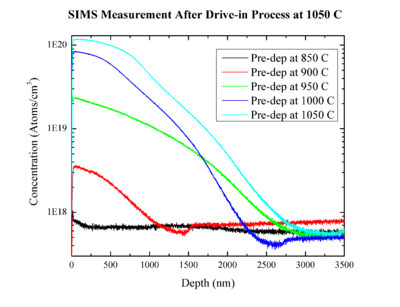
Looking at the "SIMS Measurement After Drive-in Process at 1050 oC" graph, it can be seen that the two curves "Pre-dep at 950 oC" and "Pre-dep at 1000 oC" are crossing each other, but according to the theory they should not do that. Only one wafer has been meassured, so there is not that much statistical data to verify it with.


