Specific Process Knowledge/Lithography/Coaters: Difference between revisions
| Line 493: | Line 493: | ||
|style="background:WhiteSmoke; color:black" align="center"| | |style="background:WhiteSmoke; color:black" align="center"| | ||
Silicon, III-V, and glass | Silicon, III-V, and glass | ||
No resist or crystalbond allowed in the HMDS module | |||
|- | |- | ||
|style="background:LightGrey; color:black"|Batch | |style="background:LightGrey; color:black"|Batch | ||
Revision as of 16:49, 19 May 2020
Coater Comparison Table
| Equipment | Spin Coater: Gamma UV | Spin Coater: Süss Stepper | Spin Coater: Gamma E-beam and UV | Spin Coater: RCD8 | Spin Coater: LabSpin 02 | Spin Coater: LabSpin 03 | Spin Coater: Manual All Purpose | Spray Coater | |
|---|---|---|---|---|---|---|---|---|---|
| Purpose |
|
|
|
|
|
|
| ||
| Performance | Substrate handling |
|
|
|
|
|
|
| |
| Permanent media |
|
|
|
|
Only manual dispense | Only manual dispense |
| ||
| Manual dispense option |
|
|
|
|
| ||||
| Process parameter range | Spindle speed |
|
|
|
|
|
|
||
| Gyrset |
|
|
|
|
|
|
|||
| Substrates | Substrate size |
|
|
|
|
|
|
| |
| Batch size |
|
|
|
|
|
|
| ||
| Allowed materials |
|
|
|
|
|
|
| ||
Spin coating
The process of spin coating consists of a selection of the following steps:
- Priming (typically HMDS)
- Acceleration to a low spin speed if dynamic dispense is used
- Resist dispense (static or dynamic)
- Resist spreading at low spin speed
- Spin-off
- Backside rinse (typically during spin-off)
- Edge-bead removal
- Softbake (contact or proximity)
After priming, the wafer is centered on the coater chuck and held in place by vacuum, or in some cases pins. If static dispense is used, the wafer remains static during the ensuing resist dispense. In the case of dynamic dispense, the wafer rotates at low spin speed during the dispense. Using too high spin speed during dispense can cause surface wetting issues, while a too low spin speed causes the resist to flow onto the backside of the wafer. After dispense, a short spin at low spin speed may be used in order to spread the resist over the wafer surface before spin-off.
Spin-off
The spin-off cycle determines the thickness of the resist coating. For a given resist, the thickness is primarily a function of the spin-off speed and the spin-off time, both following an inverse power-law (y=k*x^-a). The acceleration to the spin-off speed also influences the thickness, but the effect is dependent on previous steps. The spin-off is usually a simple spin at one speed, but it may be comprised of several steps at different spin speeds. After spin-off, the wafer is decelerated.
The coated thickness, t, as a function of the spin-off speed, w, follows an inverse power-law, t = k * w-a. The constant, k, is a function of the resist viscosity and solid content, and the spin-off time. The exponent, a, is dependent on solvent evaporation, and is typically ~½ for UV resists. This means that from the thickness t1 achieved at spin speed w1, one can estimate the spin speed w2 needed to achieve thickness t2 using the relation:
t1*w1½ = t2*w2½ => w2 = w1 * t12/t22.
For thick SU-8, however, a is observed to be ~1 (probably due to the low solvent content and/or the formation of skin). In this case, the relation simply becomes:
t1*w1 = t2*w2 => w2 = w1 * t1/t2.
Backside rinse
Dependent on the spin speeds used in the various steps of the spin coating, resist may creep over the edge of the wafer and onto the backside. Also, some resists tend to leave fine strings of resist protruding from the edge of the wafer, or folded onto the backside, an effect sometimes referred to as "cotton candy". This resist will contaminate the softbake hotplate, and thus subsequent wafers with resist. In a backside rinse step, solvent administered through a nozzle to the backside of the wafer while spinning at low or medium spin speed dissolves the resist and washes it away. After the rinse, a short spin at medium spin speed dries the wafer before the softbake. During the backside rinse solvent inevitably creeps onto the front side of the wafer. This effect may be used to dissolve and subsequently remove an edge-bead, but it may also leave the rim of the wafer exposed. As an alternative to backside rinse, a wafer which is left dirty on the backside by the spin coat process may be softbaked in proximity in order to protect the hotplate from contamination. This leaves front side coating intact, but also leaves the backside dirty.
Edge bead
During spin coating, resist builds up at the edge of the wafer due to the change in surface tension at the edge. This phenomenon is called an edge-bead. Dependent on spin coating parameters, the coating may be several times thicker at the edge than in the central area. In a subsequent hard contact exposure step, this edge-bead induces an undesired proximity gap which reduces the lateral resolution, and may even cause the wafer to stick to the mask.
In an edge-bead removal step, solvent administered through a nozzle positioned at the edge of the wafer while spinning at low or medium spin speed dissolves the resist and washes it away. After the removal, a short spin at medium spin speed dries the wafer before the softbake. Dependent on the viscosity (solvent content) of the resist at the point of edge-bead removal, this drying spin may cause the resist to re-flow and create a secondary edge-bead. In some cases, it may be necessary to (partially) softbake the resist before edge-bead removal.
Softbake
After spin coating, the solvent in the resist formulation must be evaporated in a baking step in order to solidify the resist. This softbake can be carried out as a contact bake or a proximity bake. In a contact bake, the wafer is held in close contact to the hotplate surface while resting on shallow bumps only 150µm above the hotplate. In a proximity bake, the wafer is first moved into proximity, e.g. 1mm, of the hotplate surface, then held there (on the lift pins) for the duration of the bake.
Spin coaters at DTU Nanolab
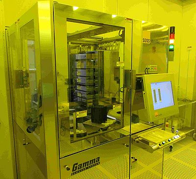
Spin Coater: Gamma UV
Feedback to this section: click here
Spin Coater: Gamma UV was installed at DTU Nanolab in March 2015. It is a Gamma 2M cluster from Süss MicroTec with spin coating, vapour priming, and baking modules. The system handles 4" and 6" wafers without size conversion, and can be set up to handle 2" or 8".
The coater is equipped with 3 different resists lines:
- AZ MiR 701
- AZ nLOF 2020
- AZ 5214E
and
- 1 syringe, which can be used for various resists.
The processes that are available on the system are developed by Nanolab. Upon request, it is possible to establish new processes. Use of the syringe requires special training, and would as a starting point require batches in excess of 20 wafers.
The user manual, quality control procedures and results, user APVs, and contact information can be found in LabManager
Process information
| Purpose |
| |
|---|---|---|
| Resist |
| |
| Performance | HMDS contact angle |
60 - 80° |
| Coating thickness |
| |
| Process parameters | Priming temperature |
120 °C |
| Spin speed |
10 - 6000 rpm | |
| Spin acceleration |
10 - 10000 rpm/s | |
| Hotplate temperature |
25 - 200 °C | |
| Cool plate temperature |
21 °C | |
| Substrates | Substrate size |
|
| Allowed materials |
Silicon and glass No resist or crystalbond allowed in the HMDS module | |
| Batch |
1 - 25 |
1) Requires tool change.
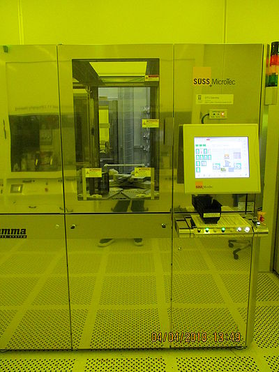
Spin Coater: Gamma E-beam and UV
Feedback to this section: click here
Spin Coater: Gamma E-beam and UV will be installed at DTU Nanolab in June 2017. It is a Gamma 4M cluster from Süss MicroTec with spin coating, vapour priming, and baking modules. The system handles 2", 4", and 6" wafers without size conversion, using two separate coater stations.
The 2" coater station is equipped with 2 different resists lines:
- AZ 5214E
- AR-P 6200.09 (CSAR)
and
- 1 syringe, which can be used for various resists (anisole or PGMEA-based).
The 4"/6" coater station is equipped with 4 different resists lines:
- AZ 5214E
- AZ MiR 701
- AR-P 6200.09 (CSAR)
- AZ 4562
The processes that are available on the system are developed by Nanolab. Upon request, it is possible to establish new processes. Use of the syringe requires special training, and would as a starting point require batches in excess of 20 wafers.
Training video (for Spin Coater: Gamma UV)
The user manual, quality control procedures and results, user APVs, and contact information can be found in LabManager
Process information
- Quality Control (QC)
- HMDS
- AZ 5214E on Coater1 and Coater2
- AZ MiR 701 on Coater2
- CSAR on Coater1 and Coater2
- AZ 4562 on Coater2
- Edge bead removal on Coater1 and Coater2
| Purpose |
| |
|---|---|---|
| Resist |
| |
| Performance | HMDS contact angle |
60 - 80° (on Silicon) |
| Coating thickness |
| |
| Process parameters | Priming temperature |
120 °C |
| Spin speed |
10 - 6000 rpm | |
| Spin acceleration |
10 - 10000 rpm/s | |
| Hotplate temperature |
25 - 200 °C | |
| Cool plate temperature |
21 °C | |
| Substrates | Substrate size |
|
| Allowed materials |
Silicon, III-V, and glass No resist or crystalbond allowed in the HMDS module | |
| Batch |
1 - 25 |
Spin Coater: RCD8
Feedback to this section: click here
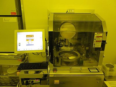
Spin Coater: RCD8 is a model RCD8 T spin coater from Süss MicroTec with a motorized media arm and Gyrset functionality. It's primary purpose is spin coating of SU-8 resist. However, due to the possibility of using a non-vacuum chuck, the spin coater is also suitable for coating of substrates with e.g. textured backsides or membranes.
The user manual, user APV, and contact information can be found in LabManager
Process information
| Purpose |
| |
|---|---|---|
| Resist |
| |
| Performance | Coating thickness |
|
| Process parameters | Spin speed |
Vacuum chuck: 10 - 5000 rpm |
| Spin acceleration |
10 - 3000 rpm/s | |
| Substrates | Substrate size |
|
| Allowed materials |
All cleanroom materials ? | |
| Batch |
1 |
Manual Spin Coaters
Go back to Coater comparison table.
| Purpose | Labspin |
Spin coating of resist ONLY in dedicated bowlsets Please do NOT use substances which is not for the dedicated bowlsets |
|---|---|---|
| All purpose |
Spin coating of dirty substances in All purpose
| |
| Process parameters | Spin speed |
|
| Spin acceleration |
| |
| Substrates | Substrate size |
|
| Allowed materials |
All cleanroom materials Please ONLY use substances which is for the dedicated bowlsets in labspins | |
| Batch |
1 |
|
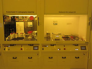
|
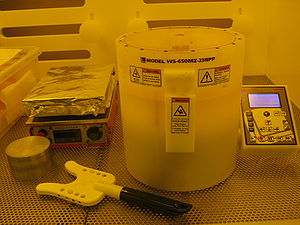
|
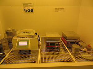
| Spin Coater: Labspin 02 | Spin Coater: Labspin 03 + fumehood 11 | Spin Coater: Manual All Purpose |
| Loacted in wetbench 08 in E-5 | Located in wetbench 09 in E-5 | Located in fumehood in C-1 |
| LabSpin 6, Süss MicroTec | LabSpin 6, Süss MicroTec | WS-650, Laurell |
| LabManager | LabManager | LabManager |
Training video: LabSpin02 + 03
Process information
Spin curves (LabSpin 6): AZ 5214E, AZ nLOF 2020, ZEP 520A, FOX-15, AZ 4562, CSAR 6200
