Specific Process Knowledge/Etch/IBE⁄IBSD Ionfab 300/IBE magnetic stack etch
Feedback to this page: click here
The work on this page was done Kristian Hagsted Rasmussen, DTU Nanolab, unless otherwise stated
Etching magnetic stacks
Magnetic stacks can be etched or more precisly milled in the Ion Beam Etcher (IBE). Below is presented some work done on milling stacks of magnetic layers.
Results of Design of Experiments optimization of magnetic stack etching (Kristian Hagsted Rasmussen@nanotech.dtu.dk spring 2011)
Process parameters
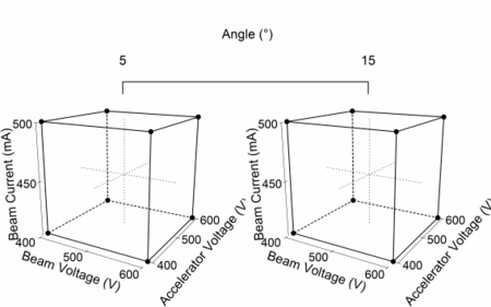
To find the optimal parameters, Design of Experiments was applied with the intervals shown on the figure below. The final optimized recipe is listed in the table.
| Parameter | Optimized etch | DoE low value | DoE high value | |
|---|---|---|---|---|
| Neutalizer current [mA] | 450 | 450 | 550 | |
| RF Power [W] | 800 | - | - | |
| Beam current [mA] | 400 | 400 | 500 | |
| Beam voltage [V] | 500 | 400 | 600 | |
| Beam accelerator voltage | 500 | 400 | 600 | |
| Ar flow to neutralizer [sccm] | 5.0 | - | - | |
| Ar flow to beam [sccm] | 10.0 | - | - | |
| Rotation speed [rpm] | 20 | - | - | |
| Stage angle [degrees] | 5 | 5 | 15 | |
| Helium backside cooling [Torr] | 37.5 | - | - |
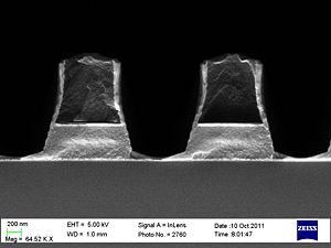
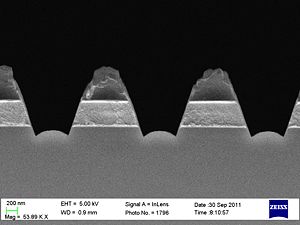
Some SEM profile images of the etched stacks
For a good pattern transfer with IBE a large amount of redeposition on the resist edge has been observed. To reduce this redeposition the best option seems to be to use a photo resist just thick enough for the wanted etch depth. An alternative is sidewall sputtering at low incident angle. However experiments have shown poor cleaning rate and for narrow structures low angles will give rise to shadowing effects.
Endpoint detection with SIMS
End point detection is achieved by SIMS, and the etch rate is approximately 25 Nm/min.
Problems with resists stripping after etching
Resist stripping after the etch can be hard due to burned resist, to remedy this try to lower the current. Changing the currect will chance the sidewall angle and new studies of etch profiles will be necessary. For help, discussion and further info please contact Kristian Hagsted Rasmussen or the dry etch group [1].
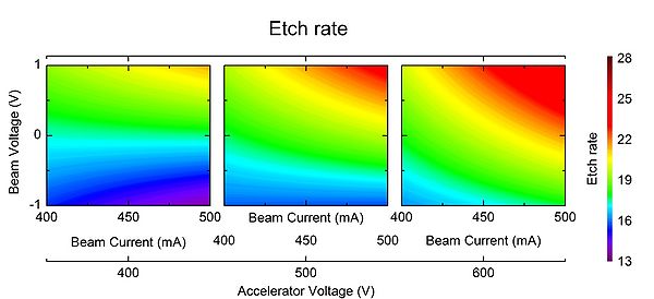
Design of Experiment results
The etch rate and corner angle are dependent on several parameters each. Below two graphs showing these dependencies are shown. Note that the values are fitted and may not represent the actual value after etch, however feel free to use the graphs to estimate the values for your test run.
Conclusions
- Etch rate around 20 nm/min with optimized recipe.
- Good feature definition after etch.
- Good end point detection by SIMS.
- Burned resist: Lower current, 300 mA can limit resist burning. Note this will affect pattern transfer.
- Hare ears (also called fences) due to redeposition, thinner resist can limit the size.


