LabAdviser/Technology Research/Presentation Form/Process flow form
Jump to navigation
Jump to search
Below is shown the form when making process flows. The tables can be copied and the content edited so it fits the process flow you need to make. It is important that you link to the page and sections in LabAdviser where you have documented the process development you have made in your project.
1 Thermal oxidation
| Step | Description | LabAdviser link | Image showing the step | |
|---|---|---|---|---|
| 1.1 | Si wafer | Start with a 100 mm Si<100> wafer that is single side polished and p doped with boron. This will be the absorber in the final solar cell. | Wafer information, types of avaliable wafers are listed. | |
| 1.2 | RCA clean | The wafer has to be RCA cleaned, before entering an oxidation furnace. | RCA cleaning, the different steps in the cleaning procedure are described. | |
| 1.3 | SiO2 dry oxidation | Grow a dry thermal oxide layer in the Boron Drive-in furnace (A1). The oxide layer will be patterned later on to define n-doped areas ("electron membrane".) | Boron Drive-in furnace, info about performance and process parameter range. | |
2 Lithography and oxide etch
| Step | Description | LabAdviser link | Image showing the step | |
|---|---|---|---|---|
| 2.1 | HMDS surface treatment | To ensure the resist sticks to the surface, the wafer is HMDS treated before resist spining. | HMDS oven | |
| 2.2 | Spin resist on wafer backside | The backside of the wafer needs to be protected, to prevent the SiO2 from being etched in the first etch step (section 3). | Resist spinners. Information about what resists that can be used with the spinners. | |
| 2.3 | Spin resist on wafer frontside | The frontside of the wafer is covered with a resist layer. | Information about resist processing, positive and reversed lithography processes. | |
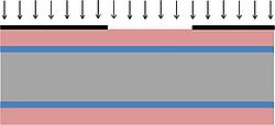
| 2.4 | Expose photoresist in aligner | The resist layer on the wafer frontside is exposed in the aligner, with a dark field mask. Align the mask to wafer flat, and use hard contact. | Aligner-6inch - EVG620. Here you can see a comparison between different aligners. | |
| 2.5 | Develop photoresist | In the development step the exposed resist is removed, so that a resist pattern is formed on the surface. | Development, standard development times are listed. | |
| 2.6 | Optical microscope inspection | Check the results of the exposure and development with an optical microscope by inspecting that the pattern and alignment marks are clearly visible. Right image: top view of alignment marks. The alignment marks will be used to align the wafer to the mask in next lithography step (section 5). | The different optical microscopes and their features are listed. | |


