LabAdviser/Technology Research/Organic Ice Resists for Electron-Beam Lithography - Instrumentation and Processes
Feedback to this page: click here
Organic Ice Resists for Electron-Beam Lithography - Instrumentation and Processes
- Project type: Ph.D. project
- Project responsible: William Tiddi (DTU Orbit)
- Supervisors: Assoc. Prof. Marco Beleggia, Assist. Prof. Anpan Han
- Partners involved: DTU Danchip/Cen
- Full thesis: Link
- Overview: Electron-Beam Lithography on Organic Ice Resists
- Overview: SEM-LEO Customizations for Organic Ice Resists
Project Description

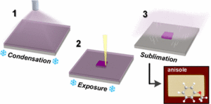
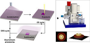
Fabrication of micro- and nanostructures, the building blocks of modern electronics and nanotechnology, requires one or more lithography iterations where the desired geometries are defined in a sacrificial layer, the resist, to be transferred into a functional material. A typical lithography process involves multiple different instruments, engineered materials and abundant solvents to create, develop, and then remove the thin resist film patterns on the desired substrate. In Ice Lithography, instead, the role of resist is played by a thin frozen water film: deposition, patterning and transfer happen without harmful chemicals, in a single tool, even on non-planar or fragile substrates, therefore bypassing limitations of conventional techniques.
This PhD project takes this promising technique to the next level. We recreated an ice lithography setup by modifying a scanning electron microscope for cryogenic operations and ice deposition. We then explored a variety of ices as resists and developed a novel approach to electron beam lithography which uses elementary organic molecules as resist: the chosen chemical is condensed from its vapour phase at cryogenic temperature to form a thin frozen layer which demonstrates resist-like capabilities.
The approach proved suitable for a variety of organic ices: isopropanol, anisole, nonane, 1-pentanol. Further work focused on the two most suitable candidates, nonane and anisole. Using our custom instrument, we patterned on samples as thin as 5 nm and as small as just 2 mm across. We realized arrays of 100-nm-wide silicon nanowires with an aspect ratio of 4, 100 nm patterns on suspended silicon nitride membranes for transmission electron microscopy, and proof-of-concept quantum devices based on 1-mm2 arrays of sub-micron diamond nanopillars. The lithography steps can be iterated multiple times for more complex patterning configurations and multilayer stacks, with the sample never having to leave the tool in-between: this gives further versatility to the technique, opening a pathway towards true 3D electron beam lithography with functional materials.
We explored, characterized and optimized this novel technology in detail to make it accessible to the broader nanotechnology community. The entire lithography requires no other tool and uses trivial amounts of readily available precursor material; at the same time performances in terms of dose and resolution are comparable to established resists, and the resulting features are directly compatible with established processes developed for resist-based pattern transfer.
Dissemination
Publications in Peer Reviewed Journals
- Organic Ice Resists
- Link to Article
- W. Tiddi, A. Elsukova, H. T. Le, P. Liu, M. Beleggia, and A. Han
Nano Letters, vol. 17, pp. 7886-7891, 2017.

- Organic ice resists for 3D electron-beam processing - Instrumentation and operation
- Link to Article
- W. Tiddi, A. Elsukova, M. Beleggia, and A. Han
Microelectronic Engineering, vol. 192, pp. 38-43, 2018.

- Inductively coupled plasma nanoetching of atomic layer deposition alumina
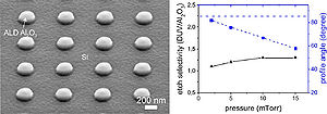
- Link to Article
- A. Han, B. Chang, M. Todeschini, H. T. Le, W. Tiddi and M. Keil
Microelectronic Engineering, vol. 193, pp. 28-33, 2018.

Published Patents
- A METHOD FOR CREATING STRUCTURES OR DEVICES USING AN ORGANIC ICE RESIST.
- Link to Patent Database
- A. Han (Inventor), W. Tiddi (Inventor), M. Beleggia (Inventor)
IPC No.: B29C 67/ 00 A I. Patent No.: WO2017191079. Nov 09, 2017.
Conferences and Workshops Contributions
- Organic ice resists - condensed small molecules as spin-free volatile E-beam resists
- W. Tiddi, A. Elsukova, H. T. Le, M. Beleggia, and A. Han
Oral presentation at 43rd International conference on Micro and Nano Engineering, Braga, Portugal, 2017.
- Ice lithography - ice-based nanopatterning
- W. Tiddi
Workshop lecture at Nordic Nanolab User Meeting 2017, Trondheim, Norway, 2017.
- Advances in Ice Lithography in Denmark and China
- W. Tiddi, D. Zhao, M. Qiu, M. Beleggia, and A. Han
Abstract and Poster at 42nd International conference on Micro and Nano Engineering, Vienna, Austria, 2016.
- Ice lithography - water-based nanopatterning.
- W. Tiddi, M. Beleggia, and A. Han
Abstract and Poster at Sustain-ATV Conference 2016, Kgs. Lyngby, Denmark, 2016.
- Proximity Effects in a Chemically Amplified Electron Beam Resist Patterned at 100 keV.
- W. Tiddi, T. Greibe, M. Beleggia, and A. Han
Abstract and Poster at 41st International conference on Micro and Nano Engineering, The Hague, Netherlands, 2015.
Ice Lithography

Physical dimension of integrated circuits keep shrinking at exponential rates, due market demand for faster, more powerful, longer-lasting and more compact electronic devices. Standard fabrication techniques manage to keep up the pace, but need to resort to extremely expensive equipment, increased fabrication complexity and intense research for dedicated chemicals satisfying the tightening process constraints.
Ice lithography is a nanopatterning technique derived from electron beam lithography, showing feature resolution below 10nm. A thin water ice layer condensed on the sample takes the role of the lithographic resist film when exposed to electron or ion beams. This process is immensely cheaper and more sustainable than state-of-the-art techniques relying on physical masks and aggressive chemistries.
At DTU Danchip/Cen, we investigate ice lithography and the steps it needs to be ported from research to future industry, establishing its potential as the break-through technology needed to advance further in the ultra large scale integration semiconductor roadmap.
Want to know more?
- https://www.youtube.com/watch?v=_8OvbTUIUNs
- King, G.M. et al., 2005. Nanometer patterning with ice. Nano Letters, 5(6), 1157–1160.
- Han, A. et al., 2011. An ice lithography instrument. Review of Scientific Instruments, 82(6), 065110.
- Han, A. et al., 2012. Nanopatterning on nonplanar and fragile substrates with ice resists. Nano Letters, 12(2), 1018–1021.