LabAdviser/314/Microscopy 314-307/Postprocessing/Lattice fringes
Feedback to this page: click here
(content by Jakob Birkedal Wagner @DTU Nanolab, March 2020)
Analysis of lattice fringe images (HRTEM) using Digital Micrograph
The resolution of transmission electron microscopy (TEM) allows for retrieving crystallographic information from the lattice fringe micrographs acquired. In general, the atomic columns are not directly images in the micrographs due to aberrations in the objective lens, but the lattice fringes spacings found in the images are directly related to atomic lattice spacings as well as the symmetries found in the images is directly correlated to the symmetries found in the crystal structure imaged.
The digital micrographs can be analyzed using various image processing tools. Here, we focus on the dedicated micrograph analysis tool named Digital Micrograph. This program is also used to acquire TEM images on most of DTU Nanolab’s TEMs.
An off-line version of Digital Micrograph (GMS3) can be found here (free Windows version): GATAN Digital Micrograph
Choose the Si Viewer license.
Example of analysis of lattice fringe image
This little walkthrough will show a few ways of measuring lattice space distances in a lattice fringe image in Digital Micrograph.
Lattice spacing in real space
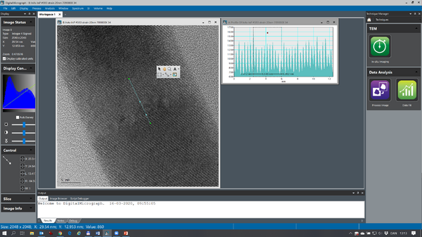
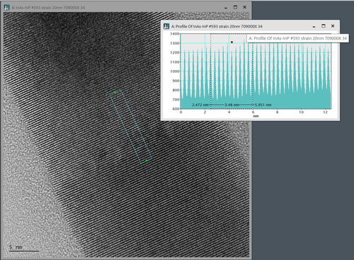
This image show a nice lattice fringe image of a InAs/InP nanowire. The distance of the lattice fringes running perpendicular to the nanowire direction can be measured by ‘right clicking’ on the image and choose the ‘profile’ icon (the ‘wavy’ icon below ‘A’ in the image. The you draw a line in the image and an intensity profile turns up. You can measure the distance of interest in the profile view. In this example 10 lattice space distances are measured to increase the measurement precision (d=3.54nm/10 = 3.54Å). If your image is a bit noisy the intensity profile can be averaged by ‘double clicking’ on the drawn profile in the image and enter the integration width (in pixels). An example of that is shown below:
Lattice spacing in reciprocal space
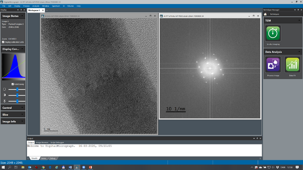
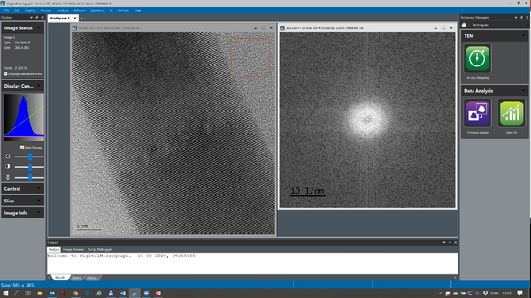
At times, it is easier to measure lattice space distances using Fast Fourier Transforms (FFTs). With the image of interest as active press Ctrl F in order to get an FFT of the image (see below):
The complex FFT is by default shown as the logarithm of the modulus. The FFT is calibrated so it is possible to measure the lattice space distances directly by measuring the distance between the dominant Fourier components.
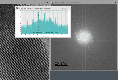
Here the distance between the Fourier components representing the same lattice space distance as analyzed above measured. The distance is d*=5.59 nm-1, which can be coverted by taking the reciprocal value: d=2/d*=2/5.59nm-1=3.58Å (here 2 reciprocal lattice space distances are measured, hence the ‘2’ in the calculation. The slight difference is due to the precision in the measurements and that the FFT here measures an average value over the image, while the direct space methods in this case is more local.
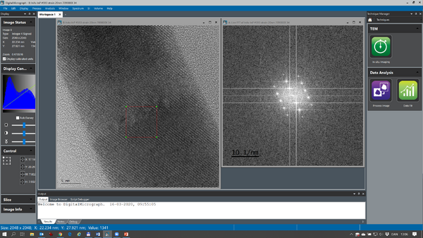
In order to get FFTs from smaller parts of the acquired micrograph, you have to define a region of interest (ROI) before you calculate the FFT:
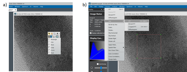
‘Right click’ on your image and choose the ‘Rectangle ROI’ tool (a). Mark the region of interest while holding down the ‘shift’ key. This way the ROI is restricted to a square making the FFT analysis more intuitive. After you have marked the ROI choose ‘Live FFT’ from the drop down menu (b). Now the outline of the ROI should become red. Now it is possible to move the ROI around the micrograph while following the FFT ‘live’:
