Specific Process Knowledge/Lithography

From LabAdviser
Jump to navigation Jump to search


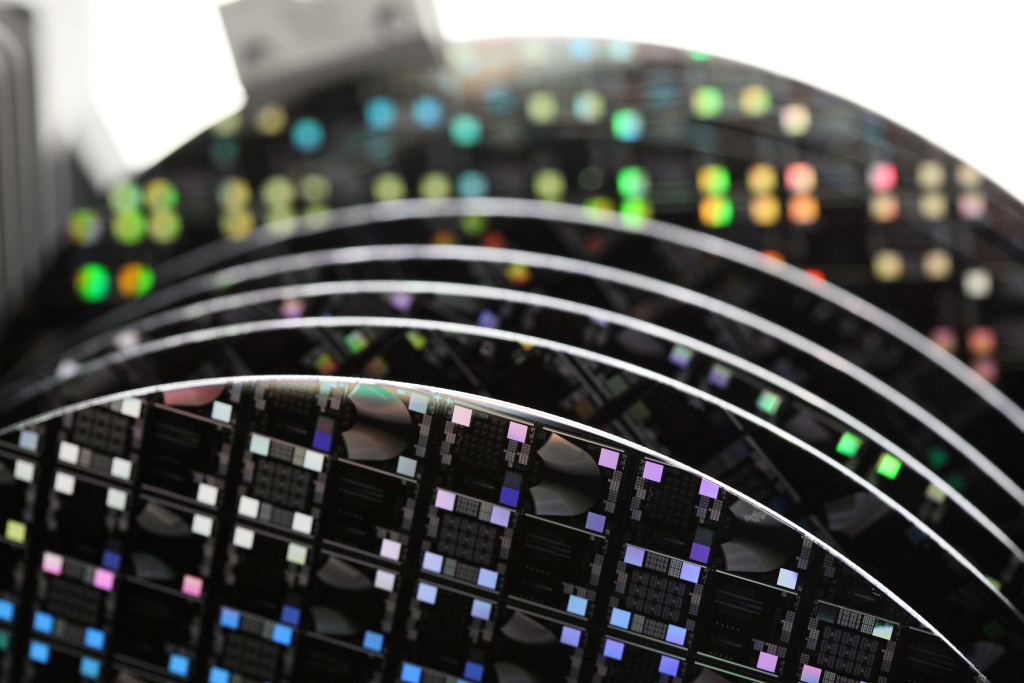
DUV wafers.jpg

Feedback to this page: click here


Comparing lithography methods at DTU Danchip

UV Lithography DUV Stepper Lithography E-beam Lithography Nano Imprint Lithography 2-Photon Polymerization Lithography Section under construction.jpg
Generel description Pattern transfer via UltraViolet (UV) light Pattern transfer via DeepUltraViolet (DUV) light Patterning by electron beam Pattern transfer via hot embossing(HE) Direct writing via IR laser
Pattern size range
  • ~1.25 µm and up
  • ~200 nm and up
  • ~12 nm - 1 µm
  • ~20 nm and up
  • 3D voxel through transparent substrate: 0.3 µm diameter; 0.6 µm high
  • 2D spot on opaque substrate: 0.6 µm diameter
Resist type
  • UV sensitive:
    • AZ 5214E, AZ 4562, AZ MiR 701 (positive)
    • AZ 5214E, AZ nLOF 2020, SU-8 (negative)
  • DUV sensitive
    • JSR KRF M230Y, JSR KRF M35G (positive)
    • UVN2300-0.8 (negative)
  • E-beam sensitive
    • AR-P6200 CSAR, ZEP502A , PMMA, HSQ, mr-EBL, AR-N 7520
  • Imprint polymers:
    • Topas
    • PMMA
  • UV sensitive:
    • IP photoresists, SU-8 (3D)
    • AZ resists (2D)
Resist thickness range

~0.5µm to 20µm

~50nm to 2µm

~30nm to 0.5 µm

~ 100nm to 2µm

droplet or coating

Typical exposure time

2s-30s pr. wafer

Process depended, depends on pattern, pattern area and dose

Depends on dose, Q [µC/cm2], beam current, I [A], and pattern area, A [cm2]: t = Q*A/I

Process depended, depends also on heating and cooling temperature rates

Process depended, depends on pattern and dose

Substrate size
  • small samples
  • 50 mm wafers
  • 100 mm wafers
  • 150 mm wafers
  • 100 mm wafers
  • 150 mm wafers
  • 200 mm wafers

We have cassettes that fit to

  • 4 small samples (20mm, 12mm, 8mm, 4mm)
  • 6 wafers of 50 mm in size
  • 2 wafers of 100 mm in size
  • 1 wafer of 150 mm in size

Only one cassette can be loaded at time

  • small samples
  • 50 mm wafers
  • 100 mm wafers
  • 150 mm wafers
  • Cover slides
  • 50 mm wafers
  • 100 mm wafers
  • IBIDI
Allowed materials
  • Any standard cleanroom material
  • Any standard cleanroom material
  • Any standard cleanroom material
  • Any standard cleanroom material
  • Any standard cleanroom material


Equipment Pages

Pretreatment

Coaters

UV Exposure

Electron Beam Exposure

Deep-UV Exposure

Baking

Development

Strip

Lift-off

NanoImprint Lithography

3D Lithography


Training

THIS SECTION IS UNDER CONSTRUCTIONUnder construction.png