Specific Process Knowledge/Etch/Etching of Silicon Oxide/SiO2 etch using ASE/More test with CF4/H2, CHF3 and C4F8/H2 - SiO2 etch: Difference between revisions

From LabAdviser
Jump to navigation Jump to search
Line 152: Line 152:
<br clear="all" />
<br clear="all" />
<br>
<br>
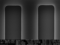
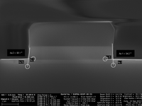
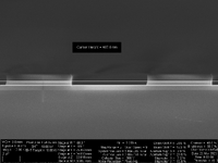
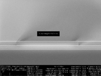
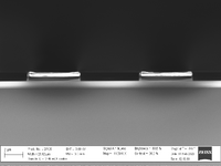
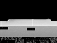
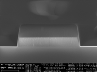
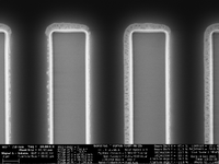
===Recipes and results - <span style="background:#FFD850">CHF<sub>3</sub> tests===
{| border="1" cellspacing="1" cellpadding="1"  align="left"
! '''Recipe'''
! '''Recipe parameters'''
! '''Process time'''
! '''Date'''
! '''SEM picture'''
! '''SEM pic w/ no resist'''
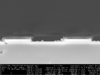
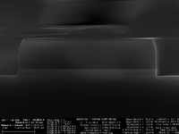
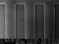
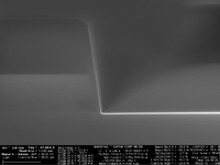
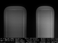
! '''Redeposition - top view'''
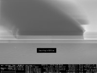
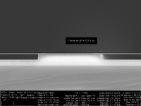
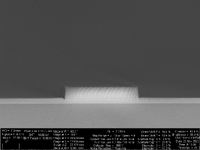
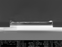
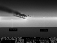
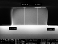
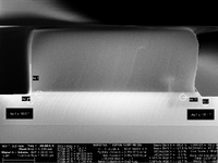
! '''Profile angles'''
! '''Etch rate in SiO2'''
! '''Etch rate in resist <br> (AZ5214E inverse)'''
! '''Selectivity <br> (SiO2:resist)'''
! '''Etch rate in Si'''
|-
|-
|-style="background:white; color:black"
|<!-- '''Recipe name''' --> CHF3_t1
|<!-- '''SiO2 before etch''' --> CHF<sub>3</sub>= '''22.5''' sccm <br> Coil= 800W <br> Platen= 15W <br> Press= 2.5mTorr <br> Temp= 20°C <br>
|<!--'''Process time'''--> 12:00 min
|<!--'''Date'''--> 04/09/2023
|<!--'''SEM picture'''--> [[File:CHF3 t1 pat C 01.png|200px]]
|<!--'''SEM pic w/ no resist'''-->
|<!--'''Redeposition - top view'''--> [[File:CHF3 t1 12min af PA 03.png|200px]]
|<!--'''Profile angles'''-->
|<!--'''Etch rate in SiO2'''--> 69.7 nm/min <br> +/- 10.5%
|<!--'''Etch rate in resist'''--> 57.3 nm/min <br> +/- 12.9%
|<!--'''Selectivity (SiO2:resist)'''--> 1.22
|<!--'''Etch rate in Si'''-->
|-
|-
|-style="background:white; color:black"
|<!-- '''Recipe name''' --> '''CHF3_t2'''
|<!-- '''SiO2 before etch''' --> CHF<sub>3</sub>= 22.5 sccm <br> Coil= '''150W''' <br> Platen= '''25W''' <br> Press= 2.5mTorr <br> Temp= 20°C <br>
|<!--'''Process time'''--> 25:00 min
|<!--'''Date'''--> 04/09/2023
|<!--'''SEM picture'''--> [[File:CHF3 t2 pat C 05.png|200px]]
|<!--'''SEM pic w/ no resist'''-->
|<!--'''Redeposition - top view'''--> [[File:CHF3 t2 25min af PA 05.png|200px]]
|<!--'''Profile angles'''--> [[File:CHF3 t2 pat C 03.png|200px]]
|<!--'''Etch rate in SiO2'''--> 26.7 nm/min <br> +/- 11.9%
|<!--'''Etch rate in resist'''--> 24.2 nm/min <br> +/- 21.1%
|<!--'''Selectivity (SiO2:resist)'''--> 1.1
|<!--'''Etch rate in Si'''-->
|-
|-
|-style="background:white; color:black"
|<!-- '''Recipe name''' --> '''CHF3 t2'''
|<!-- '''SiO2 before etch''' --> CHF<sub>3</sub>= 22.5 sccm <br> '''H<sub>2</sub>= 22.5 sccm''' <br> Coil= 150W <br> Platen= 25W <br> Press= 2.5mTorr <br> Temp= 20°C <br>
|<!--'''Process time'''--> 10:00 min
|<!--'''Date'''--> 22/09/2023
|<!--'''SEM picture'''--> [[File:CHF3.t2-10H2-25min-C-01.png|200px]]
|<!--'''SEM pic w/ no resist'''-->
|<!--'''Redeposition - top view'''--> [[File:CHF3.t2 22.5H2 10min af PA 02.png|200px]]
|<!--'''Profile angles'''--> [[File:CHF3.t2-10H2-25min-C-08.png|200px]]
|<!--'''Etch rate in SiO2'''--> 9,7 nm/min <br> +/- 34.4%
|<!--'''Etch rate in resist'''--> 1,8 nm/min <br> +/- 46.5%
|<!--'''Selectivity (SiO2:resist)'''--> 5.4
|<!--'''Etch rate in Si'''-->
|-
|-
|-style="background:white; color:black"
|<!-- '''Recipe name''' --> CHF3_t1
|<!-- '''SiO2 before etch''' --> CHF<sub>3</sub>= '''22.5''' sccm <br> '''H<sub>2</sub>= 10''' sccm <br> Coil= 800W <br> Platen= 15W <br> Press= 2.5mTorr <br> Temp= 20°C <br>
|<!--'''Process time'''--> 10:00 min
|<!--'''Date'''--> 12/09/2023
|<!--'''SEM picture'''--> [[File:CHF310 H2 10min 08.png|200px]]
|<!--'''SEM pic w/ no resist'''-->
|<!--'''Redeposition - top view'''--> [[File:CHF310 H2 10min af PA top 01.png|200px]]
|<!--'''Profile angles'''--> [[File:CHF310 H2 10min 10.png|200px]]
|<!--'''Etch rate in SiO2'''--> 59,6 nm/min <br> +/- 12.9%
|<!--'''Etch rate in resist'''--> 47,5 nm/min <br> +/- 21.5%
|<!--'''Selectivity (SiO2:resist)'''--> 1.25
|<!--'''Etch rate in Si'''-->
|-
|-
|-style="background:white; color:black"
|<!-- '''Recipe name''' --> CHF3_t1
|<!-- '''SiO2 before etch''' --> CHF<sub>3</sub>= '''22.5''' sccm <br> '''O<sub>2</sub>= 10''' sccm <br> Coil= 800W <br> Platen= 15W <br> Press= 2.5mTorr <br> Temp= 20°C <br>
|<!--'''Process time'''--> 10:00 min
|<!--'''Date'''--> 11/09/2023
|<!--'''SEM picture'''--> [[File:CHF310 O2 10min 01.png|200px]]
|<!--'''SEM pic w/ no resist'''-->
|<!--'''Redeposition - top view'''--> [[File:CHF310 O2 10min af PA top 02.png|200px]]
|<!--'''Profile angles'''--> [[File:CHF310 O2 10min 04.png|200px]]
|<!--'''Etch rate in SiO2'''--> 60,6 nm/min <br> +/- 10.1%
|<!--'''Etch rate in resist'''--> 130,8 nm/min <br> +/- 8.8%
|<!--'''Selectivity (SiO2:resist)'''--> 0.46
|<!--'''Etch rate in Si'''-->
|-
|-
|-style="background:white; color:black"
|<!-- '''Recipe name''' --> CHF3 t1
|<!-- '''SiO2 before etch''' --> CHF<sub>3</sub>= '''22.5''' sccm <br> H<sub>2</sub>= '''22.5''' sccm <br> Coil= 800W <br> Platen= 15W <br> Press= 2.5mTorr <br> Temp= 20°C <br>
|<!--'''Process time'''--> 10:00 min
|<!--'''Date'''--> 20/09/2023
|<!--'''SEM picture'''--> [[File:CHF3=22.5 H2 10min C 01.png|200px]]
|<!--'''SEM pic w/ no resist'''-->
|<!--'''Redeposition - top view'''--> [[File:CHF3.t1 22.5H2 10min af PA 02.png|200px]]
|<!--'''Profile angles'''--> [[File:CHF3=22.5 H2 10min C 03.png|200px]]
|<!--'''Etch rate in SiO2'''--> 47,3 nm/min <br> +/- 12%
|<!--'''Etch rate in resist'''--> 26,4 nm/min <br> +/- 17,4%
|<!--'''Selectivity (SiO2:resist)'''--> 1.8
|<!--'''Etch rate in Si'''-->
|-
|-
|-style="background:white; color:black"
|<!-- '''Recipe name''' --> CHF3 t1
|<!-- '''SiO2 before etch''' --> CHF<sub>3</sub>= '''22.5''' sccm <br> H<sub>2</sub>= '''35''' sccm <br> Coil= 800W <br> Platen= 15W <br> Press= 2.5mTorr <br> Temp= 20°C <br>
|<!--'''Process time'''--> 10:00 min
|<!--'''Date'''--> 22/09/2023
|<!--'''SEM picture'''--> [[File:CHF3 35H2 10min C 02.png|200px]]
|<!--'''SEM pic w/ no resist'''-->
|<!--'''Redeposition - top view'''--> [[File:CHF3 35H2 10min af PA 01.png|200px]]
|<!--'''Profile angles'''--> [[File:CHF3 35H2 10min D 05.png|200px]]
|<!--'''Etch rate in SiO2'''--> 36,5 nm/min <br> +/- 10.6%
|<!--'''Etch rate in resist'''--> 17,5 nm/min <br> +/- 13.9%
|<!--'''Selectivity (SiO2:resist)'''--> 2.09
|<!--'''Etch rate in Si'''-->
|-
|-
|-style="background:white; color:black"
|<!-- '''Recipe name''' --> CHF3 t1
|<!-- '''SiO2 before etch''' --> CHF<sub>3</sub>= '''35''' sccm <br> H<sub>2</sub>= '''35''' sccm <br> Coil= 800W <br> Platen= 15W <br> Press= 2.5mTorr <br> Temp= 20°C <br>
|<!--'''Process time'''--> 10:00 min
|<!--'''Date'''--> 22/09/2023
|<!--'''SEM picture'''--> [[File:CHF3 3535H2 10min E 01.png|200px]]
|<!--'''SEM pic w/ no resist'''-->
|<!--'''Redeposition - top view'''--> [[File:CHF3 35.35H2 10min af PA 01.png|200px]]
|<!--'''Profile angles'''--> [[File:CHF3 3535H2 10min C 06.png|200px]]
|<!--'''Etch rate in SiO2'''--> 42 nm/min <br> +/- 15.4%
|<!--'''Etch rate in resist'''--> 23,8 nm/min <br> +/- 22.2%
|<!--'''Selectivity (SiO2:resist)'''--> 1.76
|<!--'''Etch rate in Si'''-->
|-
|-
|-style="background:white; color:black"
|<!-- '''Recipe name''' --> CHF3 t1
|<!-- '''SiO2 before etch''' --> CHF<sub>3</sub>= 22.5 sccm <br> '''CF<sub>4</sub>= 22.5''' sccm <br> Coil= 800W <br> Platen= 15W <br> Press= 2.5mTorr <br> Temp= 20°C <br>
|<!--'''Process time'''--> 10:00 min
|<!--'''Date'''--> 22/09/2023
|<!--'''SEM picture'''--> [[File:CHF3.t1 22.5CF4 10min C 01.png|200px]]
|<!--'''SEM pic w/ no resist'''-->
|<!--'''Redeposition - top view'''--> [[File:CHF3 22.5CF4 10min af PA 01.png|200px]]
|<!--'''Profile angles'''--> [[File:CHF3.t1 22.5CF4 10min C 03.png|200px]]
|<!--'''Etch rate in SiO2'''--> 75,8 nm/min <br> +/- 13.1%
|<!--'''Etch rate in resist'''--> 74,9 nm/min <br> +/- 10.8%
|<!--'''Selectivity (SiO2:resist)'''--> 1.01
|<!--'''Etch rate in Si'''-->
|-
|-
|-style="background:white; color:black"
|<!-- '''Recipe name''' --> CHF3 t1
|<!-- '''SiO2 before etch''' --> CHF<sub>3</sub>= '''22.5''' sccm <br> H<sub>2</sub>= '''22.5''' sccm <br> Coil= 800W <br> Platen= 15W <br> '''Press= 25mTorr''' <br> Temp= 20°C <br>
|<!--'''Process time'''--> 10:00 min
|<!--'''Date'''--> 22/09/2023
|<!--'''SEM picture'''--> [[File:CHF3.t122.5H2 25mT 10m C 04.png|200px]]
|<!--'''SEM pic w/ no resist'''-->
|<!--'''Redeposition - top view'''--> [[File:CHF3 22.5H2 25mT 10mn af PA 01.png|200px]]
|<!--'''Profile angles'''--> [[File:CHF3.t122.5H2 25mT 10m C 03.png|200px]]
|<!--'''Etch rate in SiO2'''--> -
|<!--'''Etch rate in resist'''--> -
|<!--'''Selectivity (SiO2:resist)'''--> no etch done,<br> polymer deposited
|<!--'''Etch rate in Si'''-->
|-
|-
|-style="background:white; color:black"
|<!-- '''Recipe name''' --> CHF3 t1
|<!-- '''SiO2 before etch''' --> CHF<sub>3</sub>= 22.5 sccm <br> H<sub>2</sub>= 22.5 sccm <br> Coil= 800W <br> Platen= 15W <br> Press= 2.5mTorr <br> '''Temp= 0°C''' <br>
|<!--'''Process time'''--> 10:00 min
|<!--'''Date'''--> 22/09/2023
|<!--'''SEM picture'''--> [[File:CHF3-22.5-H2-10min-0C-C-03.png|200px]]
|<!--'''SEM pic w/ no resist'''-->
|<!--'''Redeposition - top view'''--> [[File:CHF3 22.5H2 10min 0C af PA 01.png|200px]]
|<!--'''Profile angles'''--> [[File:CHF3-22.5-H2-10min-0C-C-07.png|200px]]
|<!--'''Etch rate in SiO2'''--> 48 nm/min <br> +/- 11.2%
|<!--'''Etch rate in resist'''--> 23,3 nm/min <br> +/- 13.7%
|<!--'''Selectivity (SiO2:resist)'''--> 2.06
|<!--'''Etch rate in Si'''-->
|-
|-
|}
<br clear="all" />


===Recipes and results - <span style="background:#FFD850">C<sub>4</sub>F<sub>8</sub> / H<sub>2</sub> tests</span> ===

Revision as of 12:23, 14 December 2023

More test with CF4/H2, CHF3 and C4F8/H2 - SiO2 etch

Tests performed by Maria Farinha @DTU Nanolab


Recipes and results - CF4 / H2 tests
Recipe Recipe parameters Process time Date SEM picture SEM pic w/ no resist Redeposition - top view Profile angles Etch rate in SiO2 Etch rate in resist
(AZ5214E inverse)
Selectivity
(SiO2:resist)
Etch rate in Si
CF4ICP 22.5/22.5 CF4= 22.5 sccm
H2= 22.5 sccm
Coil= 800W
Platen= 15W
Press= 2.5mTorr
Temp= 20°C
11:00 min 11/09/2023 CF4ICP 11min C 01.png 800px-CF4ICP 11min af PA top 01.png 800px-CF4ICP 11min C 03.png 68 nm/min
+/- 8.5%
60,2 nm/min
+/- 9%
1.13
CF4ICP 35/10 CF4= 35 sccm
H2= 10 sccm
Coil= 800W
Platen= 15W
Press= 2.5mTorr
Temp= 20°C
08:00 min March 2023 200px-35.10 af ase 04.png 200px-35.10 af PA bot 03.png 69 nm/min
+/- 11.1%
77,1 nm/min
+/- 9.4%
0.9
CF4ICP 45/0 CF4= 45 sccm
H2= 0 sccm
Coil= 800W
Platen= 15W
Press= 2.5mTorr
Temp= 20°C
08:00 min March 2023 200px-CF4ICP 45.0c bf PA 04.png 200px-CF4ICP 45.0c af Pa-bot 06.png 71.4 nm/min
+/- 10.3%
96,5 nm/min
+/- 6.0%
0.74
CF4ICP 45/10 CF4= 45 sccm
H2= 10 sccm
Coil= 800W
Platen= 15W
Press= 2.5mTorr
Temp= 20°C
08:00 min March 2023 200px-45.10 af ASE 01.png 200px-45.10 af PA center 07.png 67.8 nm/min
+/- 14.9%
88,86 nm/min
+/- 4.8%
0.76
CF4lowCP 22.5/22.5 CF4= 22.5 sccm
H2= 22.5 sccm
Coil= 150W
Platen= 25W
Press= 2.5mTorr
Temp= 20°C
20:00 min Sept 2023 CF4lowCP 20m pat C03.png CF4owCP 20min af PA 03.png 23.8 nm/min
+/- 11%
20,6 nm/min
+/- 19.4%
1.16
CF4lowCP 35/10 CF4= 35 sccm
H2= 10 sccm
Coil= 150W
Platen= 25W
Press= 2.5mTorr
Temp= 20°C
10:00 min Feb 2023 CF4lowCP 35.10 10.png Low35 10 af PA 12.png 22.65 nm/min
+/- 10.2%
35.9 nm/min
+/- 10.1%
0.63
CF4lowCP 45/0 CF4= 45 sccm
H2= 0 sccm
Coil= 150W
Platen= 25W
Press= 2.5mTorr
Temp= 20°C
10:00 min Feb 2023 CF4lowCP.right 01.png Low45 0 af PA 05.png 24.9 nm/min
+/- 10.1%
52,3 nm/min
+/- 7.1%
0.47
CF4lowCP 45/10 CF4= 45 sccm
H2= 10 sccm
Coil= 150W
Platen= 25W
Press= 2.5mTorr
Temp= 20°C
10:00 min Feb 2023 CF4owCP 20min af PA 03.png 29,4 nm/min
+/- 13.7%
100,6 nm/min
+/- 16.5%
0.29


Recipes and results - C4F8 / H2 tests

Recipe Recipe parameters Process time Date SEM picture SEM pic w/ no resist Redeposition - top view Profile angles Etch rate in SiO2 Etch rate in resist
(AZ5214E inverse)
Selectivity
(SiO2:resist)
Etch rate in Si
SiO2_ICP C4F8= 10 sccm
H2= 28 sccm
Coil= 1000W
Platen= 100W
Press= 2.5mTorr
Temp= 20°C
04:00 min 04/09/2023 SiO2 ICP 4m pat C 07.png SiO2 ICP 4min af PA 02.png SiO2 ICP 4m pat C 04.png 211,9 nm/min
+/- 14.6%
153,4 nm/min
+/- 16.7%
1.4
SiO2_ICP C4F8= 10 sccm
H2= 28 sccm
Coil= 800W
Platen= 15W
Press= 2.5mTorr
Temp= 20°C
04:00 min 22/09/2023 SiO2 ICP 800W-15W 4min C 04.png SiO2 ICP 800.15W 4min af PA 02.png SiO2 ICP 800W-15W 4min E 04.png 134,7 nm/min
+/- 20.8%
145,7 nm/min
+/- 25.1%
0.92