LabAdviser: Difference between revisions
No edit summary |
No edit summary |
||
| (349 intermediate revisions by 16 users not shown) | |||
| Line 1: | Line 1: | ||
__notoc__ | |||
[[image:Til LA forside 2024-05-03 161145.png|right|500x500px|thumb|Photos: DTU Nanolab]] | |||
{{CC1}} | |||
<!--LabAdviser is a process handbook for equipment and processes at the cleanroom facilities and the characterisation facilities in building 314/307. The function and capacity of each piece of equipment is described and general process steps, eg photolithography procedures, are clarified. LabAdviser is meant to advise you to a good starting point for your cleanroom process for further optimization to meet your needs. To enter LabAdviser you need to '''log in with your DTU login'''. LabAdviser is only editable for DTU Nanolab employees. If you need further information about certain machinery or processes, please contact Nanolab personnel. Any feedback you might have on LabAdviser is welcome and can be given by mail to the LabAdviser mailbox: [mailto:labadviser@nanolab.dtu.dk labadviser@nanolab.dtu.dk]--> | |||
LabAdviser is a wiki designed for users of the DTU Nanolab facilities. If you are not a current user you are free to surf around, and also [https://www.nanolab.dtu.dk/english '''please take a look at our homepage''']. You can also take a [https://www.nanolab.dtu.dk/capabilities/cleanroom-3d-tour'''virtual tour of the DTU Nanolab cleanroom facility'''] or explore our [https://www.youtube.com/channel/UCJhdUTUJRDNODNiC3V95RQQ '''YouTube channel'''] with a selection of training videos. <br> | |||
[[ | |||
*'''[[/Process flow approval|Process flow approval]]''' | LabAdviser contains information about | ||
*'''[[Specific Process Knowledge]]''' | *Equipment for micro- and nanofabrication in the DTU Nanolab cleanroom facility in building 346 and surroundings (in building 346 and 347) | ||
**[[ | *Characterization equipment, primarily electron microscopy, in building 314 and 307. | ||
**[[ | *Fabrication steps in micro- and nanofabrication that take place at the cleanroom fabrication facility and surroundings; and | ||
*Electron microscopy methods that take place in building 314/307. | |||
An overview of the equipment in these facilities is given and some fabrication process flows and singles fabrication steps are described. In general LabAdviser is meant to help you find the right equipment and give you a good starting point for micro- and nanofabrication as well as for electron microscopy. This should not replace communication with the staff of the facilities but we recommend reading LabAdviser material as preparation before contacting staff. To be able to edit LabAdviser you need to '''log in with your DTU login''' (only for staff of the facilities). If you need further information about certain machinery or processes, please contact the relevant staff. Feedback and input is welcome by email to: [mailto:labadviser@nanolab.dtu.dk labadviser@nanolab.dtu.dk] | |||
<br> | |||
'''News in LabAdviser:''' <br/> | |||
<!-- *The latest LabAdviser update: [[Media:Monthly LabAdviser update 20231110.docx|LabAdviser update sent out 2023-11-10]] <br> --> | |||
*Slides from the latest Tech Forum: [https://labmanager.dtu.dk/function.php?module=PeriodicDocument&view=docs&page_id=397 Tech Forum slides in LabManager - requires login] <br/> | |||
== Contents == | |||
[[Image:Virtual tour in the clean room.JPG|right|300px|thumb|Take a virtual tour in the DTU Nanolab cleanroom [[https://www.nanolab.dtu.dk/capabilities/cleanroom-3d-tour]]]] | |||
[[Image:YouTube.JPG|right|300px|thumb|DTU Nanolab on YouTube [[https://www.youtube.com/channel/UCJhdUTUJRDNODNiC3V95RQQ]]]] | |||
*'''[[/Introduction to LabAdviser and Processing|Introduction to LabAdviser and Micro/Nano Fabrication]]''' | |||
*'''[[/Introduction to LabManager|Introduction to LabManager]]''' | |||
*'''[[/Process flow approval|Process flow template & approval]] (fabrication)''' | |||
<!-- *'''[[/CEN|Characterization in building 314/307 - OLD]] --> | |||
*'''[[/314|Characterization in building 314/307]] | |||
*'''[[Specific Process Knowledge|Micro and Nano Fabrication Overview ]]''' | |||
*'''[[/Courses |Courses (Introduction course, Tool Package Training's (TPT))]] | |||
*'''[[LabAdviser/Technology Research|Some DTU Nanolab Projects - Technology Research]]''' | |||
<!-- *'''[[/Equipment List|Equipment List]]''' --> | |||
*'''[[Surveys and statistics|Surveys, statistics, monthly LabAdviser updates and other info.]]''' | |||
*'''[[How to add information to LabAdviser]]''' | |||
<!-- | |||
*'''[[/Technology Research|Under Construction]]''' | |||
--> | |||
<br clear="all" /> | |||
==Overview of micro and nano fabrication steps - a guide to where you can find fabrication information in LabAdviser== | |||
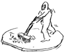
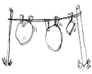
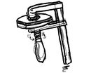
''All drawings in this section done by Jesper Hanberg @DTU Nanolab'' | |||
=== Click on [show] and see choices to the right === | |||
{| style="color: black;vertical-align:top" width="100%" border=0 cellpadding="4" cellspacing="0" | |||
| colspan="2" | | |||
|- | |||
| style="width: 50%; vertical-align:top;"| | |||
{| id="linkTable" border="1" cellpadding="0" cellspacing="0" style="text-align:center;" | |||
! class="hideImage" style="display:none"| Front Image | |||
! style="display:none"|- | |||
! style="display:none"|- | |||
! style="display:none"|- | |||
|- | |||
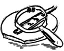
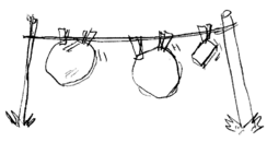
! class="hideImage" width="150" height="180px"| Clean your sample[[file:jehanClean.png|130px|frameless ]] | |||
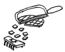
! class="hideImage" width="150" | Dry your sample [[file:jehanDry.png|130px|frameless ]] | |||
! class="hideImage" width="150" | Create a thin film on your sample [[file:jehanfilm.png|130px|frameless ]] | |||
! class="hideImage" width="150" | Dope your sample [[file:jehanDope.png|130px|frameless ]] | |||
|- | |||
! class="hideImage" width="150" height="180px"| Thermal treatment of your sample [[file:jehanThermal.png|130px|frameless ]] | |||
! class="hideImage" width="150" | Make a mask on your sample[[file:jehanmask.png|130px|frameless ]] | |||
! class="hideImage" width="150" | Transfer pattern to your sample [[file:jehanTransfer.png|130px|frameless ]] | |||
! class="hideImage" width="150" | Define your structure directly [[file:jehandefine.jpg|130px|frameless ]] | |||
|- | |||
! class="hideImage" width="150" height="180px"| Bond your samples together [[file:jehanBond.png|130px|frameless ]] | |||
! class="hideImage" width="150" | Characterize your sample [[file:jehanCharacterize.png|130px|frameless ]] | |||
! class="hideImage" width="150" | Pack your sample [[file:jehanPack.png|130px|frameless ]] | |||
! class="hideImage" width="150" | Process flow examples [[file:processflow_b.png|130px|frameless ]] | |||
|- | |||
|} | |||
| style="color:black; width: 50%; vertical-align: top;"| | |||
{| class="wikitable hideable hidden" border="1" cellspacing="0" cellpadding="0" align="left" width="400px" style="float:right;" | |||
! style="text-align:right;" | [[image:DUV6.jpg|center|400px|thumb|Photo: DTU Nanolab]] | |||
|- | |||
|} | |||
| style="color:black; width: 50%; vertical-align: top"| | |||
{| class="wikitable hideable hidden" border="1" cellspacing="0" cellpadding="0" align="left" width="430px" | |||
! colspan="3" style="text-align:left;" | [[image:Clean your sample.png|x100px|Clean your sample]] Clean your sample | |||
|- | |||
!Entry page in LabAdviser | |||
!Techniques | |||
!Materials | |||
|- | |||
|rowspan="5" valign="top" |[[Specific Process Knowledge/Wafer cleaning|Wafer cleaning]] | |||
|Soap Sonic | |||
|Removes dust and particles | |||
|- | |||
|7-up & Piranha | |||
|Removes traces of organics and alkali ions | |||
|- | |||
|RCA | |||
|Two step process to remove traces of organics and metals | |||
|- | |||
|5% HF | |||
|Removes native oxide | |||
|- | |||
|IMEC | |||
|Removing dust, traces of organics and alkali ions and slightly polish the surface. | |||
Make the surface hydrophillic | |||
|- | |||
|} | |||
{| class="wikitable hideable hidden" border="1" cellspacing="1" cellpadding="2" align="left" width="430px" | |||
!colspan="3" style="text-align:left;" | [[image:Dry your sample.png|x130px|Dry your sample]] Dry your sample | |||
|- | |||
!Entry page in LabAdviser | |||
!Techniques | |||
!Materials | |||
|- | |||
|rowspan="4" valign="top" |[[Specific Process Knowledge/Wafer and sample drying|Wafer and sample drying]] | |||
|Spin dryers | |||
|Whole wafers | |||
|- | |||
|Critial point dryer | |||
|Sensitive wafers | |||
|- | |||
|Ethanol fume drying | |||
|Sensitive wafers | |||
|- | |||
|N2 blow drying | |||
|N2 pistols | |||
|- | |||
|} | |||
{| class="wikitable hideable hidden" border="1" cellspacing="1" cellpadding="2" align="left" width="600px" | |||
!colspan="3" style="text-align:left;" | [[image:Create a film on your sample.png|x100px|Create a layer/film on your sample]] Create a layer/film on your sample | |||
|- | |||
!Entry page in LabAdviser | |||
!Techniques | |||
!Materials | |||
|- | |||
|[[Specific Process Knowledge/Thermal Process/Oxidation| Thermal Process/Oxidation]] | |||
|Thermal oxidation | |||
|Thermal SiO2 | |||
|- | |||
|rowspan="8" valign="top"|[[Specific Process Knowledge/Thin film deposition| Thin film deposition]] | |||
|Sputter deposition | |||
|Metals: Al, Ti, Cr, Co, Ni, Cu, Mo, Pd, Ag, Sn, Ta, W, Pt, Au, Fe, Mg, Nb, Ru <br> | |||
Semiconductors: Si, Ge, ZnO <br> | |||
Oxides: SiO<sub>2</sub>, ITO, TiO<sub>2</sub>, Al<sub>2</sub>O<sub>3</sub>, MgO, Ta<sub>2</sub>O<sub>5</sub> Cr<sub>2</sub>O<sub>3</sub><br> | |||
Transparent Conducting Oxides: ITO, AZO<br> | |||
Alloys: TiW, NiCr, AlTi, NiV, AlCu, CoFe, CuTi, FeMn, MnIr, NiCo, NiFe, YSZ <br> | |||
|- | |||
|Thermal evaporation | |||
|Al, Ge, Ag | |||
|- | |||
|E-beam evaporation | |||
|Metals: Ti, Cr, Al, Ni, Pt, Au, Mo, Nb, Pd, Ag, Cu, W, Ta <br> | |||
Semiconductors: Si, Ge <br> | |||
Oxides: SiO<sub>2</sub>, TiO<sub>2</sub> <br> | |||
Alloys: NiCr, TiAl | |||
|- | |||
|LPCVD | |||
|Si<sub>3</sub>N<sub>4</sub>, SRN, SiO<sub>2</sub>, Si (poly and amorph) | |||
|- | |||
|PECVD | |||
|Si<sub>3</sub>N<sub>4</sub>, SiO<sub>2</sub>, PBSG | |||
|- | |||
|MVD | |||
|FDTS | |||
|- | |||
|Electroplating | |||
|Ni | |||
|- | |||
|Epitaxial growth /MOCVD | |||
|Al, As, Ga, In, P. doping: Si, Zn | |||
|- | |||
|rowspan="2" valign="top"| [[Specific Process Knowledge/Lithography/Coaters|Lithography/Coaters]] | |||
|Spin coating | |||
|resists, polymers | |||
|- | |||
|Spray coating | |||
|resists, polymers | |||
|- | |||
|} | |||
{| class="wikitable hideable hidden" border="1" cellspacing="1" cellpadding="2" align="left" width="430px" | |||
!colspan="3" style="text-align:left;" | [[image:Dope your sample.png|x100px|Dope your sample]] Dope your sample | |||
|- | |||
|- | |||
!Entry page in LabAdviser | |||
!Techniques | |||
!Materials | |||
|- | |||
|rowspan="5" valign="top"| [[Specific Process Knowledge/Doping|Doping]] | |||
|Ion implant | |||
|e.g. P, B, As | |||
|- | |||
|[[Specific Process Knowledge/Thin film deposition/PECVD| PECVD]] | |||
|Deposition of SiO2 or Si3N4 doped with P,B and Ge | |||
|- | |||
|[[Specific Process Knowledge/Thin film deposition/Furnace LPCVD PolySilicon|LPCVD ]] | |||
|Deposition of PolySi doped with B or P | |||
|- | |||
|[[Specific Process Knowledge/Thermal Process/Dope with Boron|Predeposition and drive-in]] | |||
|Doping Silicon wafers with boron | |||
|- | |||
|[[Specific Process Knowledge/Thermal Process/Dope with Phosphorus|Predeposition and drive-in]] | |||
|Doping Silicon wafers with phosphorus | |||
|- | |||
|} | |||
{| class="wikitable hideable hidden" border="1" cellspacing="1" cellpadding="2" align="left" width="430px" | |||
!colspan="3" style="text-align:left;" | [[image:Thermal treat your sample.png|x100px|Thermal treatment of your sample]] Thermal treatment of your sample | |||
|- | |||
!Entry page in LabAdviser | |||
!Techniques | |||
!Materials | |||
|- | |||
|rowspan="5" valign="top"|[[Specific Process Knowledge/Thermal Process|Thermal Process]] | |||
|Annealing (>350C) | |||
|Si, PECVD layers, Al, BCB curing, Polymer | |||
|- | |||
|Oxidation | |||
|Si wafers | |||
|- | |||
|Doping with B/P | |||
|Si wafers | |||
|- | |||
|Pyrolysis | |||
|Resists: AZ, SU8, PDMS | |||
|- | |||
|Rapid Thermal Anneal (RTP) | |||
|SiO2, Si3N4, Ti, III-V | |||
|- | |||
| | |||
[[Specific Process Knowledge/Lithography/Baking| Lithography/Baking]] <br> | |||
|Baking (<300dg) | |||
|baking resist and polymers | |||
|- | |||
|} | |||
{| class="wikitable hideable hidden" border="1" cellspacing="1" cellpadding="2" align="left" width="430px" | |||
!colspan="3" style="text-align:left;" | [[image:Make a mask on your sample.png|x100px|Make a mask on your sample]] Make a mask on your sample | |||
|- | |||
!Entry page in LabAdviser | |||
!Techniques | |||
!Materials | |||
|- | |||
|rowspan="5" valign="top"|[[Specific Process Knowledge/Lithography| Lithography]] | |||
|Pattern design & Mask fabrication | |||
| | |||
|- | |||
|Photolithography | |||
|UV resists | |||
|- | |||
|Deep UV lithography | |||
|DUV resists | |||
|- | |||
|E-beam lithography | |||
|E-beam resists | |||
|- | |||
|Imprinting | |||
|Polymers | |||
|- | |||
|} | |||
{| class="wikitable hideable hidden" border="1" cellspacing="1" cellpadding="2" align="left" width="430px" | |||
!colspan="3" style="text-align:left;" | [[image:Transfer mask pattrn to your sample.png|x100px|Transfer mask pattern to your sample]] Transfer mask pattern to your sample | |||
|- | |||
!Entry page in LabAdviser | |||
!Techniques | |||
!Materials | |||
|- | |||
|rowspan="2" valign="top"|[[Specific Process Knowledge/Etch| Etch]] | |||
|Wet etch | |||
|Si, Glass, SiO2, Si3N4, Al, Cr, Ti, Au, Pt, InP, InGaAsP, GaAs/AlGaAs | |||
|- | |||
|Dry etch | |||
|Any material | |||
|- | |||
|[[Specific Process Knowledge/Lithography/LiftOff| Lithography/Lift-off]] | |||
|Lift-off | |||
|Most materials | |||
|- | |||
|} | |||
{| class="wikitable hideable hidden" border="1" cellspacing="1" cellpadding="2" align="left" width="430px" | |||
!colspan="3" style="text-align:left;" | [[image:Define your structure directly.png|x100px|Define the structure directly on your sample]] Define your structure directly | |||
|- | |||
!Entry page in LabAdviser | |||
!Techniques | |||
!Materials | |||
|- | |||
|rowspan="5" valign="top"|[[Specific Process Knowledge/Direct Structure Definition|Direct Structure Definition]] | |||
|Polymer Injection molding | |||
|Topas, PP, PE, PS | |||
|- | |||
|LASER micro machining | |||
|Silicon, Metal, Graphene (on silicon), Glass (Pyrex, fused silica), TOPAS, PMMA | |||
|- | |||
|Dicing saw | |||
|Silicon, Glass (Pyrex, fused silica) | |||
|- | |||
|[[Specific Process Knowledge/Imprinting|Imprinting]] | |||
|TOPAS, PMMA | |||
|- | |||
|Hot Embosser | |||
|Topas, PP, PE, PS, PC, PMMA, ... | |||
|- | |||
|[[Specific Process Knowledge/Lithography|Lithography definition]] | |||
|SU8, AZ resists | |||
|- | |||
|} | |||
{| class="wikitable hideable hidden" border="1" cellspacing="1" cellpadding="2" align="left" width="430px" | |||
!colspan="3" style="text-align:left;" | [[image:Bond your samples together.png|x100px|Bond your samples together]] Bond your samples together | |||
|- | |||
!Entry page in LabAdviser | |||
!Techniques | |||
|- | |||
|rowspan="3" valign="top"|[[Specific Process Knowledge/Bonding|Bonding]] | |||
|Eutectic bonding | |||
|- | |||
|Fusion bonding | |||
|- | |||
|Anodic bonding | |||
|- | |||
|[[Specific_Process_Knowledge/Etch/DryEtchProcessing/Bonding |Etch/DryEtchProcessing/Bonding]] | |||
|Temporary bonding of wafers or chips for dry etching | |||
|- | |||
|} | |||
{| class="wikitable hideable hidden" border="1" cellspacing="1" cellpadding="2" align="left" width="430px" | |||
!colspan="3" style="text-align:left;" | [[image:Characterize your sample.png|x100px|Characterize your sample]] Characterize your sample | |||
|- | |||
!Entry page in LabAdviser | |||
!What do you need to measure? | |||
!Technique/Method | |||
|- | |||
|rowspan="12" valign="top"|[[Specific Process Knowledge/Characterization|Characterization]] | |||
|Sample Imaging, XY dimensions | |||
|Microscopy: optical, SEM, AFM | |||
|- | |||
|Sample Topography | |||
|AFM, Profiling with stylus or optical | |||
|- | |||
|Film thickness and optical constants | |||
|Ellipsometry, Reflectometry, Prism Coupling | |||
|- | |||
|Film Stress | |||
|Profiling with stylus or optical | |||
|- | |||
|Wafer thickness | |||
|Micrometer gauge | |||
|- | |||
|Element analysis | |||
|XPS, EDX, SIMS | |||
|- | |||
|Contact Angle | |||
|Drop shape analyzing | |||
|- | |||
|Resistivity | |||
|Four point probe, Probe station | |||
|- | |||
|Doping level/Carrier density | |||
|ECV (Electrochemical Capacitance-Voltage) -profiler | |||
|- | |||
|Direct Bandgap | |||
|Photoluminescence | |||
|- | |||
|Lattice mismatch | |||
|X-ray diffractometer | |||
|- | |||
|Defects/contamination | |||
|Particle/defect counter | |||
|- | |||
|} | |||
{| class="wikitable hideable hidden" border="1" cellspacing="1" cellpadding="2" align="left" width="430px" | |||
!colspan="3" style="text-align:left;" | [[image:Pack your sample (back-end).png|x100px|Pack your sample (back-end)]] Pack your sample (back-end) | |||
|- | |||
!Entry page in LabAdviser | |||
!Techniques | |||
|- | |||
|rowspan="3" valign="top"|[[Specific Process Knowledge/Back-end processing|Back-end processing]] | |||
|Chip/die mounting | |||
|- | |||
|Wire bonding | |||
|- | |||
|Dicing | |||
|- | |||
|} | |||
{| class="wikitable hideable hidden" border="1" cellspacing="1" cellpadding="2" align="left" width="430px" | |||
!colspan="3" style="text-align:left;" | Process flow examples | |||
|- | |||
!Entry page in LabAdviser | |||
!Topic | |||
|- | |||
|[[LabAdviser/Introduction_to_LabAdviser_and_Processing|Introduction to LabAdviser and Processing]] | |||
|Solar cell flow | |||
|- | |||
|[[Process_flow_approval|Process flow approval]] | |||
|Info on process flow review | |||
|- | |||
|[[Specific Process Knowledge/Lithography/UVLithography#Resist Overview|UV Lithography#Resist Overview]] | |||
|UV Lithography flows | |||
|- | |||
|[[Specific Process Knowledge/Lithography/EBeamLithography#E-beam resists and Process Flows|EBeamLithography#E-beam resists and Process Flows]] | |||
|E-beam lithography flows | |||
|- | |||
|} | |||
|- | |||
|} | |||
---- | |||
<br> | |||
== Contact Information for the DTU Nanolab fabrication part == | |||
{{DanchipInfo}} | |||
<!-- The template called DanchipInfo has the address: | |||
http://labadviser.nanolab.dtu.dk/index.php/Template:DanchipInfo --> | |||
---- | |||
<br clear="all"/> | |||
==DTU Nanolab Fabrication Cleanroom Naming and Phone Numbers== | |||
===Cleanroom building 346 ground floor=== | |||
{| style="color: black;" width="100%" | |||
| colspan="2" | | |||
|- | |||
| style="width: 50%"| | |||
{| style="color: black;" width="100%" | |||
| colspan="2" | | |||
|- | |||
| style="width: 40%"| | |||
[[image:Cleanroom_naming_2017.jpg|500px|thumb|Drawing: DTU CAS Digital]] | |||
|} | |||
| style="width: 50%"| | |||
{|border="1" cellspacing="1" cellpadding="1" style="text-align:left;" | |||
|- | |||
|- | |||
|-style="background:silver; color:black" | |||
!Room number | |||
!Where in the room | |||
!Phone number | |||
|- | |||
|- | |||
|-style="background:WhiteSmoke; color:black" | |||
!A-1 | |||
|At III-V RIE | |||
|55 804 | |||
|- | |||
|- | |||
|-style="background:LightGrey; color:black" | |||
!Ax2 | |||
|At the Lesker | |||
|55 815 | |||
|- | |||
|- | |||
|-style="background:WhiteSmoke; color:black" | |||
!A-5 | |||
|In the corner near the furnace/plasma asher | |||
|55 803 | |||
|- | |||
|- | |||
|-style="background:LightGrey; color:black" | |||
!B-1 | |||
|In the corridor | |||
|55 806 | |||
|- | |||
|- | |||
|-style="background:WhiteSmoke; color:black" | |||
!C-1 | |||
|At the corridor | |||
|55 808 | |||
|- | |||
|- | |||
|-style="background:LightGrey; color:black" | |||
!D-1 | |||
|The entrance room | |||
|55 703 | |||
|- | |||
|- | |||
|-style="background:WhiteSmoke; color:black" | |||
!D-3 | |||
|At the KOH | |||
|55 940 | |||
|- | |||
|- | |||
|-style="background:LightGrey; color:black" | |||
!E-1 | |||
|By the e-beam computers | |||
|55 943 | |||
|- | |||
|- | |||
|-style="background:WhiteSmoke; color:black" | |||
!E-5/E-4 | |||
|By the MLAs in E-5, by mask aligner in E-4 | |||
|55 946 | |||
|- | |||
|- | |||
|-style="background:LightGrey; color:black" | |||
!E-6 | |||
|Furnace 6" | |||
|55 948 | |||
|- | |||
|- | |||
|-style="background:WhiteSmoke; color:black" | |||
!F-1 | |||
|III-V growth | |||
|55 949 | |||
|- | |||
|- | |||
|-style="background:LightGrey; color:black" | |||
!F-2 | |||
|To the right of the XRD and Ellipsometer | |||
|55 941 | |||
|- | |||
|- | |||
|-style="background:WhiteSmoke; color:black" | |||
!F-3 | |||
|DUV Stepper | |||
|55 947 | |||
|- | |||
|- | |||
|-style="background:LightGrey; color:black" | |||
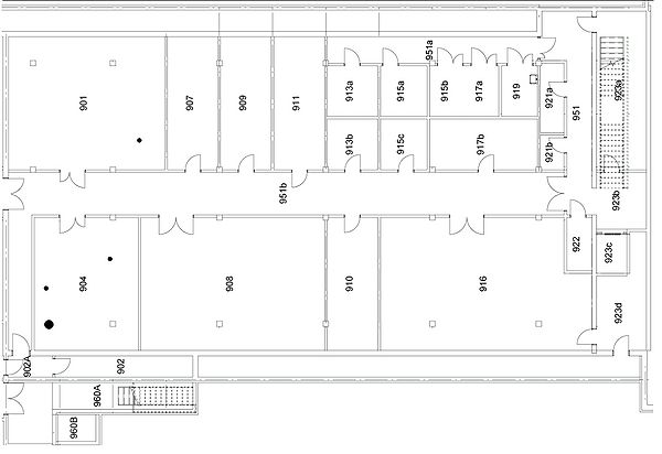
!Basement 901 | |||
|Injection molder room in the basement | |||
|55 812 | |||
|- | |||
|-style="background:LightGrey; color:black" | |||
!Basement 904 | |||
|To the right of the AFM | |||
|55 813 | |||
|- | |||
|} | |||
|} | |||
<br clear="all" /> | |||
===Basement building 346 phase 1=== | |||
[[File:Basement 346 phase 1.jpg|left|600px|thumb|Drawing: DTU CAS Digital]] <br> | |||
<br clear="all" /> | |||
==DTU Nanolab building 314 and Phone Numbers== | |||
{| style="color: black;" width="100%"; "text-align: center | |||
| colspan="2" | | |||
|- | |||
| style="width: 50%"| | |||
{| style="color: black;" width="100%" | |||
| colspan="2" | | |||
|- | |||
| style="width: 40%"| | |||
[[File:CEN building.jpg|600px|left|thumb|Drawing: DTU CAS Digital]] | |||
|} | |||
| style="width: 50%"| | |||
{| style="color: black;" width="100%" | |||
| colspan="2" | | |||
|- | |||
| style="width: 50%"| | |||
{| style="color: black;" width="100%" | |||
| colspan="2" | | |||
|- | |||
| style="width: 40%"| | |||
|} | |||
| style="width: 50%"| | |||
{|border="1" cellspacing="1" cellpadding="1" style="text-align:left;" | |||
|- | |||
|- | |||
|-style="background:silver; color:black" | |||
!Room number | |||
!Description | |||
!Phone number | |||
|- | |||
|- | |||
|-style="background:WhiteSmoke; color:black" | |||
!314-011 | |||
|QFEG 200 Cryo ESEM | |||
|56 406 | |||
|- | |||
|- | |||
|-style="background:LightGrey; color:black" | |||
!314-014 | |||
|Tecnai T20 | |||
|56 407 | |||
|- | |||
|- | |||
|-style="background:WhiteSmoke; color:black" | |||
!314-032 | |||
|Prep room 1 | |||
|No phone | |||
|- | |||
|- | |||
|-style="background:LightGrey; color:black" | |||
!314-034 | |||
|AFEG 250 ESEM | |||
|56 414 | |||
|- | |||
|- | |||
|-style="background:WhiteSmoke; color:black" | |||
!314-037 | |||
|Titan ETEM | |||
|56 418 | |||
|- | |||
|- | |||
|-style="background:LightGrey; color:black" | |||
!314-040 | |||
|Prep room 2 (Bio) | |||
|56 413 | |||
|- | |||
|- | |||
|-style="background:WhiteSmoke; color:black" | |||
!314-042 | |||
|Titan ATEM | |||
|56 409 | |||
|- | |||
|- | |||
|-style="background:LightGrey; color:black" | |||
!314-060 | |||
|Nova NanoSEM 600 | |||
|56 412 | |||
|- | |||
|- | |||
|-style="background:WhiteSmoke; color:black" | |||
!314-061 | |||
|Helios Nanolab | |||
|56 411 | |||
|- | |||
|} | |||
|} | |||
<br clear="all" /> | |||
Latest revision as of 15:13, 1 November 2024

Unless otherwise stated, this page is written by DTU Nanolab internal
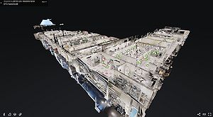
LabAdviser is a wiki designed for users of the DTU Nanolab facilities. If you are not a current user you are free to surf around, and also please take a look at our homepage. You can also take a virtual tour of the DTU Nanolab cleanroom facility or explore our YouTube channel with a selection of training videos.
LabAdviser contains information about
- Equipment for micro- and nanofabrication in the DTU Nanolab cleanroom facility in building 346 and surroundings (in building 346 and 347)
- Characterization equipment, primarily electron microscopy, in building 314 and 307.
- Fabrication steps in micro- and nanofabrication that take place at the cleanroom fabrication facility and surroundings; and
- Electron microscopy methods that take place in building 314/307.
An overview of the equipment in these facilities is given and some fabrication process flows and singles fabrication steps are described. In general LabAdviser is meant to help you find the right equipment and give you a good starting point for micro- and nanofabrication as well as for electron microscopy. This should not replace communication with the staff of the facilities but we recommend reading LabAdviser material as preparation before contacting staff. To be able to edit LabAdviser you need to log in with your DTU login (only for staff of the facilities). If you need further information about certain machinery or processes, please contact the relevant staff. Feedback and input is welcome by email to: labadviser@nanolab.dtu.dk
News in LabAdviser:
- Slides from the latest Tech Forum: Tech Forum slides in LabManager - requires login
Contents
- Introduction to LabAdviser and Micro/Nano Fabrication
- Introduction to LabManager
- Process flow template & approval (fabrication)
- Characterization in building 314/307
- Micro and Nano Fabrication Overview
- Courses (Introduction course, Tool Package Training's (TPT))
- Some DTU Nanolab Projects - Technology Research
- Surveys, statistics, monthly LabAdviser updates and other info.
- How to add information to LabAdviser
Overview of micro and nano fabrication steps - a guide to where you can find fabrication information in LabAdviser
All drawings in this section done by Jesper Hanberg @DTU Nanolab
Click on [show] and see choices to the right
Contact Information for the DTU Nanolab fabrication part
In order to get the quickest response to training requests, process approvals, questions etc. please use the following mailboxes to DTU Nanolab (formerly known as Danchip).
| Subject | Description | |
| Training and Process Flow | training@nanolab.dtu.dk | All requests regarding equipment training and process flows. Please add your Name to the subject line. Note: Requests are commonly answered within 2 workdays. |
| E-beam training | e-beam@nanolab.dtu.dk | Requests regarding training on JEOL JBX-9500FSZ or Raith Eline e-beam systems. Please study the material on the EBL Labadviser pages beforehand. |
| E-beam Cassette loading | e-beamload@nanolab.dtu.dk | Requests regarding cassette loading on JEOL JBX-9500FSZ. |
| General inquiries | nanolabsupport@nanolab.dtu.dk | Inquiries related to machines, cleanroom access, Mask review, tool changes, and others. Please add your Name to the subject line. Note: Requests are commonly answered within 2 workdays. |
| Metal Wishes | metal@nanolab.dtu.dk | Requests for change of metal in Thin Film Deposition equipment. See current and future materials in statuslog of the respective machines.
|
| Gas-related Requests | DCH-Gas@nanolab.dtu.dk | All topics gas-related (issues, information regarding ordering, delivery, changing etc). Mostly for internal DTU Nanolab use. |
| LabAdviser Mailbox | labadviser@nanolab.dtu.dk | Any questions or feedback to LabAdviser. |
| Commercial Inquiries | sales@nanolab.dtu.dk | For all inquiries regarding in-sourcing, commercial applications, rent of cleanroom space, etc |
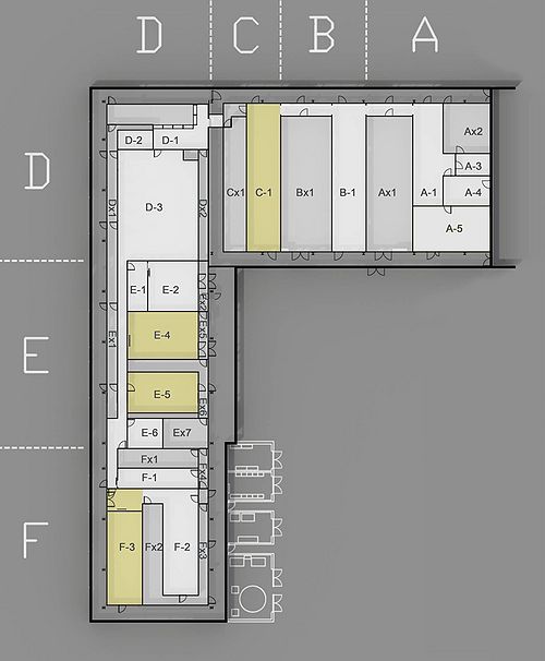
DTU Nanolab Fabrication Cleanroom Naming and Phone Numbers
Cleanroom building 346 ground floor
|
| |||||||||||||||||||||||||||||||||||||||||||||||||||
Basement building 346 phase 1
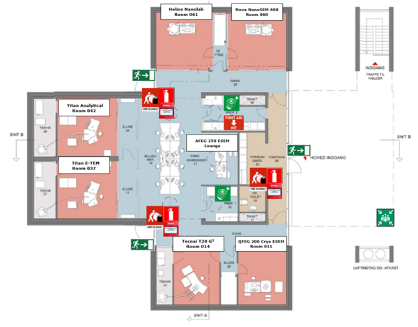
DTU Nanolab building 314 and Phone Numbers
|
|
||||||||||||||||||||||||||||||||||||||||

