Specific Process Knowledge/Thin film deposition/Deposition of Chromium/Thermal evaporation of Cr in Thermal evaporator
Feedback to this page: click here
This page is written by Evgeniy Shkondin @DTU Nanolab if nothing else is stated.
All images and photos on this page belongs to DTU Nanolab.
The fabrication and characterization described below were conducted in 2020 by Evgeniy Shkondin. The shield design was developed by Henrik Nielsen (Nanolab, ThinFilm), and built by Nanolab Facility service.
Thermal evaporation of Chromium
Chromium can be thermally evaporated in the Thermal Evaporator (NANO 36 THERMAL EVAPORATOR SYSTEM). At DTU Nanolab, for the Cr thermal source we have experimented with Cr pellets in a W boat as well as dedicated 4" long chromium plated tungsten rods (supplier: KJLC).
The process and resulting material characteristics described on this page were done using the Cr plated W rod. However, we have found that using Cr pellets is easier in the long run as it does not require modifying the chamber layout. So the current method you will most likely use is evaporation of Cr pellets from a boat (2025). There will be some differences from what is described below, e.g., uniformity will be different. You can still use the results from XRD/XRR, XPS, SEM, and AFM as an indication of what you might expect and as a guide for relevant investigations.
Cr evaporation from Cr-coated W rod
During power ramp up, the material warms up and sublimates. Unlike deposition of Al and Ag, where simple crucibles are used with point-source evaporation from bottom to the substrate, the deposition of chromium from a coated rod proceeds in all directions. To prevent the deposition on the side-walls and the bottom of the chamber a specific protecting shield is mounted beneath the tungsten rod.
The shield design was developed by Henrik Nielsen (Nanolab, ThinFilm), and build by Nanolab Facility service. The process was developed and tested by Evgeniy Shkondin (Nanolab, ThinFilm) in december 2020.
-
 Figure 1. View of Chromium deposition process from the coated tungsten rod.
 -
 Figure 2. Deposition rate is very stable through the whole process.


Set-up and installation of the rod
The deposition of Chromium requires a major change of the tool hardware installation. Ask Nanolab responsible employee if you need to perform this change.
-
 Figure 3. Cr coated rod should be mounted by squeezing it between specific clamps as shown on the image. The used rod have to be discarded.
 -
 Figure 4. Tools that needs to be used to change hardware configuration.
 -
 Figure 5. Photography of the prepared set-up.
 -
 Figure 6. Photography of the prepared set-up.
 -
 Figure 7. Photography of the prepared set-up.


Recipe and process performance
| Deposition rate (Å/s) | 1* |
|---|---|
| Maximum Thickness | 100 nm** |
| Film Tooling | 173 % |
| Density | 7.2 g/cm3 |
| Z-factor | 0.305 |
* The deposition rate can be increased (up to 2Å/s or even 5 Å/s), but it requires a new recipe.
**Although it is possible to deposit 100 nm, we do not recommend exceeding the thickness setpoint above 80 nm, due to instabilities at the end.
Deposition of 100 nm
The adjusted tooling factor 173%. Full 6" wafer is loaded with shadow-mask. No rotation. Deposition thickness setpoint is set to 100 nm.
Pressure fluctuations during the ramp-up:
- Rise 1 phase @ 0-15W: 4.4 10-6 Torr → 6.2 10-6 Torr
- Soak 1 phase @ 15W: 6.2 10-6 Torr → 10-5 Torr → 6.5 10-6 Torr
- Rise 2 phase @ 15-24W: 6.5 10-6 Torr → 1.3 10-5 Torr → 1.6 10-6 Torr
- Soak 2 phase @ 24W: 1.6 10-6 Torr → 1.8 10-6 Torr
| Pressure (Torr) | Deposition rate (Å/s) | Output power (W) | Deposited thickness (nm) | Comment |
|---|---|---|---|---|
| 2.3 10-6 | 1.0 | 24.5 | 0 | fine |
| 9.2 10-7 | 0.97 | 25 | 10 | fine |
| 8.8 10-7 | 0.98 | 25.6 | 20 | fine |
| 9.9 10-7 | 0.98 | 26.0 | 30 | fine |
| 1.2 10-6 | 0.99 | 26.3 | 40 | fine |
| 1.3 10-6 | 1.0 | 26.6 | 50 | fine |
| 1.4 10-6 | 0.99 | 26.7 | 60 | fine |
| 1.4 10-6 | 0.99 | 26.8 | 70 | fine |
| 1.4 10-6 | 1.03 | 26.6 | 80 | fine |
| 1.6 10-6 | 0.97 | 25.7 | 90 | Cr retraction starts from the center point of the rod |
| 2.5 10-6 | 1.02 | 27.4 | 100 | (10% opened area) Pressure fluctuates a little the last 10 nm. |

At the end of the lifetime (deposition in the range of 80-100nm at the given rate and set-up conditions) the Cr starts to detract from the tungsten rod leaving an empty area that illuminates a very bright light. It is not always that the retraction begins from the middle, there are cases where it starts from one of the edges. In such a case, the deposition is a bit unstable in terms of measured power and pressure.
-
 Figure 9. Cr retraction from the tingsten rod at the end of lifetime.

The limited amount of chromium, the nature of deposition (in all directions) and retruction sets a limit on how thick layer can be deposited. We do not recomend to exeed the thickness above 80 nm, and do not allow thicknesses above 100 nm.
Note! Remember to discard the used tungsten rods. Never reinstall them. Always mount a new source.
Film characterisation
Full 6" wafer is loaded for film characterization. Measured base pressure before start 4.4 10-6 Torr. Waited 1 hour before start. Deposition thickness setpoint is set to 100 nm. The prepared sample was cleaved into small pieces for characterization.
X-ray reflectivity method
XRR measurements for Cr film has been performed using Rigaku XRD SmartLab diffractometer.
-
 Figure 10. XRR scan. Substrate: Silicon 6" wafer with native oxide.

The following model is selected for XRR fitting: Native chromium oxide, bulk chromium layer, native silicon oxide, and the bulk silicon substrate. Fitting results presented in the table.
| Layer name | Thickness (nm) | Density (g/cm3) | Roughness (nm) |
|---|---|---|---|
| CrOx | 4.636 | 4.95362 | 3.107 |
| Cr | 101.6 |
6.38 | 2.5 |
| SiO2 | 1.02 | 2.19147 | 0.5 |
| Si | 2.33 | 0.02 |
In-Plane X-ray diffraction
In-Plane diffraction spectrum acquired with Rigaku XRD SmartLab diffractometer. Incident angle o IS=0.1mm, RS1=RS2=open. Scan speed: 1o/min.
The diffraction pattern reveal a polycrystalline film with a strong <111> orientation peak.
-
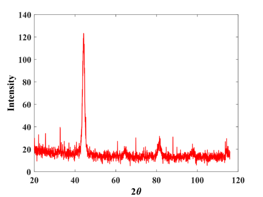 Figure 11. In-Plane XRD scan. Substrate: Silicon 6" wafer with native oxide.

X-ray photoelectron spectroscopy
XPS profiles for Cr films has been obtained using XPS K-Alpha equipment.
-
 Figure 12. Survey scan of Cr thin film after 580 s. Ar+ sputtering. Substrate: Silicon 6" wafer with native oxide.
 -
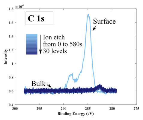 Figure 13. High resolution of C 1s signal. At the surface native airborne carbon can be observed, the signal disappears immediately after the ion beam is turned on. Substrate: Silicon 6" wafer with native oxide.
 -
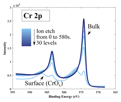 Figure 14. High resolution Cr 2p signal during the depth profiling. Ar+ sputtering proceeds from 0 to 580 s, with 20 s. interval with mid-current and energy of 3000 eV. At the surface, the Cr peak is doubled due the bonding to oxygen and bonding to Cr. After the etching the peak responsible to oxygen bonding becomes neglible. Substrate: Silicon 6" wafer with native oxide.
 -
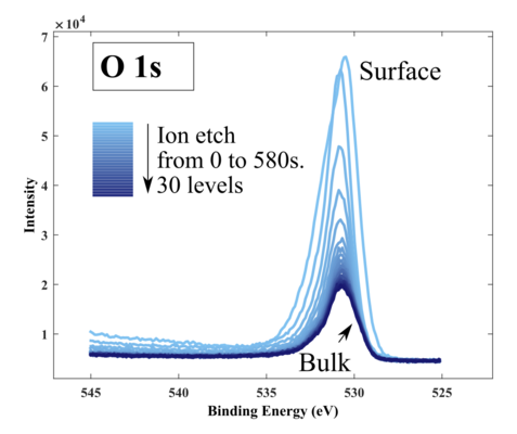 Figure 15. High resolution of O 1s signal. The signal is obviously strong at the beginning, since the top layer is composed of CrOx, but it never completely disapears, but it becomes saturated, which means that some level of oxygen is always present. Substrate: Silicon 6" wafer with native oxide.
 -
 Figure 16. XPS depth profile. The top surface is oxidized, but the oxygen signal lowers, once getting deeper. Nevertheless, it remains around 10 at.% in the bulk layer. The is a strange nitrogen lower signal. The reason is unknown. Substrate: Silicon 6" wafer with native oxide.


SEM and AFM
SEM and AFM measurements illustrate surface morphology and roughness.
-
 Figure 17. SEM image. Substrate: Silicon 6" wafer with native oxide.
 -
 Figure 18. AFM image. Substrate: Silicon 6" wafer with native oxide.

