Specific Process Knowledge/Thermal Process/Dope with Boron: Difference between revisions
| (14 intermediate revisions by 3 users not shown) | |||
| Line 1: | Line 1: | ||
'''Feedback to this page''': '''[mailto:labadviser@ | '''Feedback to this page''': '''[mailto:labadviser@nanolab.dtu.dk?Subject=Feed%20back%20from%20page%20http://labadviser.nanolab.dtu.dk/index.php/Specific_Process_Knowledge/Thermal_Process/Dope_with_Boron click here]''' | ||
The concentration of boron in the | ==Doping with boron== | ||
''This section is written by DTU Nanolab internal'' | |||
The Boron Drive-in and Pre-dep furnace (A1) can be used to pre-deposit/dope silicon wafers with boron. | |||
The boron doping is done by use of boron nitride source wafers, that allows boron to diffuse into the silicon wafers. The source wafers have to be RCA1 cleaned and activated, i.e. heated up to at least 1050 <sup>o</sup>C, before the boron pre-deposition is done. The procedure for this can be found in the user manual for the A1 furnace. | |||
In the furnace, the silicon wafers are positioned in a silicon carbide boat just next to the boron nitride source wafers. The side of the silicon wafers that needs to be doped, has to point towards the source wafers. | |||
The concentration of boron in the wafers after the pre-deposition depends on the process temperature, and the doping depth profile depends of the process time. | |||
All the graphs shown on this page have been made in 2003. A this time DTU Nanolab had a furnace dedicated only for boron pre-deposition (the A2 furnace, which is now a Gate Oxide furnace). The pre-deposition processes were done at a temperature of 1125 <sup>o</sup>C and with a flow of 5 slm N<sub>2</sub> and 0.2 slm of O<sub>2</sub>. | |||
<gallery caption="Boron profiles from SIMS " widths="400px" heights="300px" perrow="3"> | <gallery caption="Boron profiles from SIMS " widths="400px" heights="300px" perrow="3"> | ||
image:borprofil_1tim.jpg|Pre-depostion for 1 hour at 1125 °C | image:borprofil_1tim.jpg|Pre-depostion for 1 hour at 1125 °C | ||
image:borprofil_6tim.jpg|Pre-depostion for 6 hour at 1125 °C | image:borprofil_6tim.jpg|Pre-depostion for 6 hour at 1125 °C | ||
image:borprofil_16tim.jpg|Pre-depostion for 16 hour at 1125 °C | image:borprofil_16tim.jpg|Pre-depostion for 16 hour at 1125 °C | ||
</gallery> | </gallery> | ||
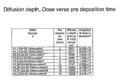
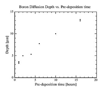
<gallery caption="Boron diffusion depth vs. pre-deposition time" widths="400px" heights="300px" perrow="3"> | <gallery caption="Boron diffusion depth vs. pre-deposition time" widths="400px" heights="300px" perrow="3"> | ||
| Line 21: | Line 30: | ||
''' | ''' | ||
== | |||
==Boron pre-deposition== | |||
''Results made by Filip Sandborg Olsen, Dec. 2015'' | ''Results made by Filip Sandborg Olsen, Dec. 2015'' | ||
| Line 29: | Line 39: | ||
''' | ''' | ||
To study the uniformity across | To study the uniformity across a wafer that has been boron doped using a pre-deposition process and a short wet oxidation to oxidize the boron phase layer in the Boron Predep and Drive-in furnace (A1) at DTU Nanolab. | ||
''' | ''' | ||
| Line 35: | Line 45: | ||
====Experimental setup==== | ====Experimental setup==== | ||
''' | ''' | ||
3 phosphorous doped device wafers (n-type) were used. In the furnace 3 RCA-cleaned wafers were placed in the center of the boat with Boron source wafers (also RCA cleaned) with the front side facing the source wafers.A pre-deposition process was made for | 3 phosphorous doped device wafers (n-type) were used. In the furnace 3 RCA-cleaned wafers were placed in the center of the boat with Boron source wafers (also RCA cleaned) with the front side facing the source wafers. A pre-deposition process was made for one hour at 1125 °C, then the source wafers were removed and the device wafers oxidized in a wet oxidation process at 950 °C for half an hour. Finally the oxide was removed in BHF and one wafer was cut into small samples for SIMS measurements. | ||
The experiment has been performed at 3 different pre-deposition times 30 min, 60 min and 90 min with and without a 30 min WET950 oxidation step. The results are resumed in the figures below. | |||
''' | ''' | ||
==== | ====Results==== | ||
''' | ''' | ||
The samples for SIMS measurements corresponds to 5 different positions on the wafer. | The samples for SIMS measurements corresponds to 5 different positions on the wafer. | ||
| Line 47: | Line 59: | ||
<br clear="all" /> | <br clear="all" /> | ||
The SIMS measurement shows a good uniformity | {| border="1" cellspacing="1" cellpadding="2" align="left" | ||
|[[image:60min_Predep_WET950.jpg|500x600px|left|thumb|SIMS Measurement at 5 different positions after pre-deposition of boron.The SIMS measurement shows a good uniformity across the wafer]]||[[image:Boron_doping_profiles.jpg|500x600px|left|thumb|SIMS Measurement for 3 different pre-deposition times 30 min, 60 min and 90 min with and without a 30 min WET950 oxidation step.]] | |||
[[image:Boron_doping_profiles | |} | ||
<br clear="all" /> | <br clear="all" /> | ||
Latest revision as of 15:58, 31 January 2023
Feedback to this page: click here
Doping with boron
This section is written by DTU Nanolab internal
The Boron Drive-in and Pre-dep furnace (A1) can be used to pre-deposit/dope silicon wafers with boron.
The boron doping is done by use of boron nitride source wafers, that allows boron to diffuse into the silicon wafers. The source wafers have to be RCA1 cleaned and activated, i.e. heated up to at least 1050 oC, before the boron pre-deposition is done. The procedure for this can be found in the user manual for the A1 furnace.
In the furnace, the silicon wafers are positioned in a silicon carbide boat just next to the boron nitride source wafers. The side of the silicon wafers that needs to be doped, has to point towards the source wafers.
The concentration of boron in the wafers after the pre-deposition depends on the process temperature, and the doping depth profile depends of the process time.
All the graphs shown on this page have been made in 2003. A this time DTU Nanolab had a furnace dedicated only for boron pre-deposition (the A2 furnace, which is now a Gate Oxide furnace). The pre-deposition processes were done at a temperature of 1125 oC and with a flow of 5 slm N2 and 0.2 slm of O2.
- Boron profiles from SIMS
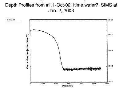
Pre-depostion for 1 hour at 1125 °C
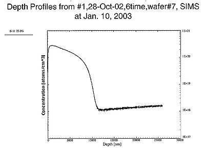
Pre-depostion for 6 hour at 1125 °C
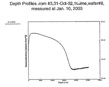
Pre-depostion for 16 hour at 1125 °C


- Boron diffusion depth vs. pre-deposition time


Boron pre-deposition
Results made by Filip Sandborg Olsen, Dec. 2015
Purpose
To study the uniformity across a wafer that has been boron doped using a pre-deposition process and a short wet oxidation to oxidize the boron phase layer in the Boron Predep and Drive-in furnace (A1) at DTU Nanolab.
Experimental setup
3 phosphorous doped device wafers (n-type) were used. In the furnace 3 RCA-cleaned wafers were placed in the center of the boat with Boron source wafers (also RCA cleaned) with the front side facing the source wafers. A pre-deposition process was made for one hour at 1125 °C, then the source wafers were removed and the device wafers oxidized in a wet oxidation process at 950 °C for half an hour. Finally the oxide was removed in BHF and one wafer was cut into small samples for SIMS measurements.
The experiment has been performed at 3 different pre-deposition times 30 min, 60 min and 90 min with and without a 30 min WET950 oxidation step. The results are resumed in the figures below.
Results
The samples for SIMS measurements corresponds to 5 different positions on the wafer.


