Specific Process Knowledge/Direct Structure Definition: Difference between revisions
Jump to navigation
Jump to search
No edit summary |
|||
| (31 intermediate revisions by 4 users not shown) | |||
| Line 1: | Line 1: | ||
'''Unless anything else is stated, everything on this page, text and pictures are made by DTU Nanolab.''' | |||
'''All links to Kemibrug (SDS) and Labmanager Including APV and QC requires login.''' | |||
'''Feedback to this page''': '''[mailto:labadviser@danchip.dtu.dk?Subject=Feed%20back%20from%20page%20http://labadviser.danchip.dtu.dk/index.php/Specific_Process_Knowledge/Characterization click here]''' | '''Feedback to this page''': '''[mailto:labadviser@danchip.dtu.dk?Subject=Feed%20back%20from%20page%20http://labadviser.danchip.dtu.dk/index.php/Specific_Process_Knowledge/Characterization click here]''' | ||
[[ | <!-- =<span style="background:#FF2800">THIS PAGE IS UNDER CONSTRUCTION</span>[[image:Under_construction.png|200px]]= --> | ||
= Direct Structure Definiton = | = Direct Structure Definiton = | ||
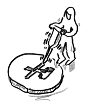
[[image:Define your structure directly.png|right|x200px|Define the structure directly on your sample]] | [[image:Define your structure directly.png|right|x200px|Define the structure directly on your sample]] | ||
By direct structure definition | By direct structure definition is meant a technique by which you create structures directly in the device material. Some of the techniques may require a master. | ||
== Choose method of structuring/equipment == | == Choose method of structuring/equipment == | ||
* [[Specific Process Knowledge/Lithography/UVLithography|UV Lithography]] | * [[Specific Process Knowledge/Lithography/UVLithography|UV Lithography]] | ||
* [[Specific Process Knowledge/Lithography/NanoImprintLithography|Nano Imprint Lithography]] | * [[Specific Process Knowledge/Lithography/NanoImprintLithography|Nano Imprint Lithography]] | ||
* [[Specific Process Knowledge/Back-end processing/Polymer Injection Molder|Polymer Injection Molder]] | * [[Specific Process Knowledge/Back-end processing/Polymer Injection Molder|Polymer Injection Molder]] | ||
* [[Specific_Process_Knowledge/Back-end_processing/Hot_Embosser|Hot Embosser]] | |||
* [[Specific Process Knowledge/Back-end processing/Laser Micromachining Tool|Laser Micromachining Tool/ablation]] | * [[Specific Process Knowledge/Back-end processing/Laser Micromachining Tool|Laser Micromachining Tool/ablation]] | ||
* [[Specific Process Knowledge/Back-end processing/Disco Saw|Dicing saw]] | * [[Specific Process Knowledge/Back-end processing/Disco Saw|Dicing saw]] | ||
<!-- | |||
== Materials for structuring == | == Materials for structuring == | ||
*Polymers | *Polymers | ||
** SU-8 | ** SU-8 | ||
*** [[Specific Process Knowledge/Lithography/UVLithography|UV Lithography]] | *** [[Specific Process Knowledge/Lithography/UVLithography|UV Lithography]] | ||
** Topas | ** Topas | ||
*** [[Specific Process Knowledge/Back-end processing/Polymer Injection Molder|Polymer Injection Molder]] | *** [[Specific Process Knowledge/Back-end processing/Polymer Injection Molder|Polymer Injection Molder]] | ||
| Line 38: | Line 43: | ||
** [[Specific Process Knowledge/Back-end processing/Disco Saw|Dicing saw]] | ** [[Specific Process Knowledge/Back-end processing/Disco Saw|Dicing saw]] | ||
**[[Specific Process Knowledge/Back-end processing/Sandblasting|Sandblasting (at DTU Nanotech).]] | **[[Specific Process Knowledge/Back-end processing/Sandblasting|Sandblasting (at DTU Nanotech).]] | ||
--> | |||
== Comparison of equipment/material == | == Comparison of equipment/material == | ||
| Line 47: | Line 53: | ||
|-style="background:silver; color:black" | |-style="background:silver; color:black" | ||
! | ! | ||
! | ![[Specific Process Knowledge/Lithography/UVLithography|UV Lithography]] | ||
! | ![[Specific Process Knowledge/Lithography/NanoImprintLithography|Nano Imprint Lithography]] | ||
![[Specific Process Knowledge/Back-end processing/Polymer Injection Molder|Polymer Injection Molder]] | |||
! | ![[Specific_Process_Knowledge/Back-end_processing/Hot_Embosser|Hot Embosser]] | ||
! | ![[Specific Process Knowledge/Back-end processing/Laser Micromachining Tool|Laser Micromachining Tool]] | ||
! | ![[Specific Process Knowledge/Back-end processing/Disco Saw|Dicing saw]] | ||
|- | |- | ||
| Line 59: | Line 65: | ||
!General description | !General description | ||
| The device is typical made in a thick film (10-100µm thick) of a polymer (SU-8) that is spun on a carrier (silicon wafer). This film is exposed through a mask and then developed and possible cured to make the polymer harder. | | The device is typical made in a thick film (10-100µm thick) of a polymer (SU-8) that is spun on a carrier (silicon wafer). This film is exposed through a mask and then developed and possible cured to make the polymer harder. | ||
| The device is typical made in a thick film (1-10µm thick) of a polymer that is spun on a carrier (silicon wafer). A master with the desired pattern is pressed into this film and the film is hardened by heating or UV-exposure. A residual layer has to be etched away by dry etching. It is possible to form very small 2½D structures over large areas relative fast. | | The device is typical made in a thick film (1-10µm thick) of a polymer that is spun on a carrier (silicon wafer). A master with the desired pattern is pressed into this film and the film is hardened by heating or UV-exposure. A residual layer has to be etched away by dry etching. It is possible to form very small 2½D structures over large areas relative fast. | ||
| The device is | | The device is typically made in Topas, PP, PE, PS or a similar polymer. A master disk, called a shim, is usually fabricated in nickel or special aluminium alloys with the desired structures to be replicated. It is mounted in the tool of the injection moulding machine. Together they form a cavity into which molten polymer is injected. It is possible to replicate both small and large 2½D structures relatively fast. Many plastic items are made by injection molding, ranging from e.g. toothbrushes to LEGO bricks. | ||
|The device is typically made using variety of different polymer foils, as well as Graphene. A master pattern, called a shim, is usually fabricated in Si, but can also be fabricated in metals as well as other polymers. It is placed inside the machine between the pressure hot plates, and using a combination of heat and pressure patterned on to the foil. It is possible to replicate both small and large 2½D structures relatively fast. | |||
| The device is made using a series of short, high intensity light pulses to engrave a pattern in almost any material. Since the light pulses are very short (100ns or 10ps) the heating of the sample can be minimized, and material can be removed without any further sample deformation/melting. | | The device is made using a series of short, high intensity light pulses to engrave a pattern in almost any material. Since the light pulses are very short (100ns or 10ps) the heating of the sample can be minimized, and material can be removed without any further sample deformation/melting. | ||
| The dicing saw is mostly used to seperate a silicon/glass wafer into individual chips. It can however also be used to make straight channels in glass/fused silica for e.g. fluidic components. | | The dicing saw is mostly used to seperate a silicon/glass wafer into individual chips. It can however also be used to make straight channels in glass/fused silica for e.g. fluidic components. | ||
| Line 68: | Line 74: | ||
|- | |- | ||
|-style="background:LightGrey; color:black" | |-style="background:LightGrey; color:black" | ||
! | !Typically used for | ||
|Optical waveguides, fluidic systems (master for PDMS/soft lithography) | |Optical waveguides, fluidic systems (master for PDMS/soft lithography) | ||
| | |?? | ||
| | |Fluidic devices, optical waveguides, surface modification. | ||
|Fluidic devices, optical waveguides, surface modification. | |Fluidic devices, optical waveguides, surface modification. | ||
|Cutting Silicon and glass wafers in odd shapes, shim cutting, shim patterning, surface modification, hole drilling in glass/silicon etc. | |Cutting Silicon and glass wafers in odd shapes, shim cutting, shim patterning, surface modification, hole drilling in glass/silicon etc. | ||
| Line 90: | Line 85: | ||
|- | |- | ||
|-style="background:WhiteSmoke; color:black" | |-style="background:WhiteSmoke; color:black" | ||
! | !Processable materials | ||
| | |||
*SU8 | |||
*AZ resists | |||
| | | | ||
* | *TOPAS | ||
* | *PMMA | ||
| | | | ||
* | *Topas 5013L-10 | ||
* | *Topas 8007S-04 | ||
* | *PS (BASF 158k) | ||
* | *Others available upon request and approval | ||
| | | | ||
* | *PMMA | ||
* | *TOPAS 5013-L10 | ||
* | *TOPAS 8007 | ||
*PC | |||
*PP | |||
*PCL | |||
*SU8 | |||
*Graphene | |||
*Metals (Al,Ni....) | |||
*For other materials contact for machine responsible personel | |||
| | | | ||
* | *Silicon | ||
* | *Metal sheets | ||
* | *Graphene (on silicon) | ||
* | *Glass (Pyrex, fused silica) | ||
* | *TOPAS | ||
*PMMA | |||
*... | |||
| | | | ||
* | *Silicon | ||
* | *Glass (Pyrex, fused silica) | ||
|- | |- | ||
| Line 122: | Line 124: | ||
|-style="background:LightGrey; color:black" | |-style="background:LightGrey; color:black" | ||
!Prerequisites | !Prerequisites | ||
| | |Sample with resist.<br> A glass mask with desired pattern. For mask layout software see [[Specific Process Knowledge/Pattern Design| Mask design]] | ||
| | |Sample with polymer.<br> A stamp with the wanted pattern, usually in Si or SiO\rm{_2} however other materials could also be used. | ||
| | |A stamp/shim with the wanted pattern, usually in Ni or Al, cut out to fit in the injection moulding machine. | ||
| | |Fabricate two blank shims (usually from aluminum foil, electroplated, nickel or milled aluminum) to protect the upper and lower press plate from polymer or other material runoff. If uniformity is an issue, the suggested procedure is to make two x PDMS foils, in order to make the force distribution as uniform as possible. The foils should be placed between the protective SHIM/CHUCK and the pressure plates. The stamp/shim with the pattern can be fabricated in variety of materials (eg. metals/polymers), using variety of different manufacturing techniques. If in doubt of which technique is right for your sample, contact for the machine responsible personel | ||
| | |||
| | |A 2D CAD model file in DXF or CONX format. [[Specific Process Knowledge/Pattern Design| Clewin5]] can convert GDS and CIF files to DXF format. | ||
|Number of lines and pitch in each direction. Your wafer. | |||
|- | |- | ||
|- | |- | ||
|-style="background:WhiteSmoke; color:black" | |-style="background:WhiteSmoke; color:black" | ||
! | !Throughput (when mask/stamp/pattern available) | ||
| | |medium: 5-10 wafers/hour depending on exposure time | ||
| | |medium: 5-10 wafers/hour depending on imprint time | ||
| | |Fast: Typically 10-300 samples/hour | ||
| | |Medium: Typically 6-15 samples/hour | ||
| | |medium-slow: 0.1-1 wafers/hour depending on pattern complexity | ||
| | |medium: ½-3 wafers/hour depending on material and # of cuts (Si cuts at 5mm/s, SiO2 at 0.5-1 mm/s) | ||
|- | |- | ||
|- | |- | ||
|-style="background:LightGrey; color:black" | |-style="background:LightGrey; color:black" | ||
! | !Min/max featuresize | ||
| | |1µm - wafer size | ||
| | |100nm - µm | ||
| | |nm - mm | ||
| | |nm - mm | ||
| | |100µm - wafer size | ||
| | |saw blade width 60µm or 200µm. Has to cut full diameter of wafer. | ||
|- | |- | ||
|- | |- | ||
|-style="background:WhiteSmoke; color:black" | |-style="background:WhiteSmoke; color:black" | ||
! | !Post-treatment | ||
| | |resist developing/baking | ||
| | |Dry Etch back (RIE), ?? Nano Imprint Lithography | ||
| | |Sprue/runner has to be broken or cut off. | ||
| | |The pressure plates must be cooled off and cleaned | ||
| | |Sample cleaning with Ultrasound etc. | ||
| | |None | ||
|- | |- | ||
|- | |- | ||
|-style="background:LightGrey; color:black" | |-style="background:LightGrey; color:black" | ||
! | !Patterning degree of freedom | ||
| | |2D | ||
| | |2D. different depths possible | ||
| | |2D. Different depths possible. | ||
| | |2D. Different depths possible. | ||
| | |2D. different depths possible | ||
| | |1D. different depths possible | ||
|- | |- | ||
|- | |- | ||
|-style="background:WhiteSmoke; color:black" | |-style="background:WhiteSmoke; color:black" | ||
! | !Sample sizes | ||
| | | | ||
| | *small samples | ||
| | *50 mm wafers | ||
| | *100 mm wafers | ||
| | *150 mm wafers | ||
| | | | ||
*small samples | |||
*50 mm wafers | |||
*100 mm wafers | |||
| | |||
*Flat disk tool: ø50mm disc | |||
*Luer tool: ø50mm disc with 12 Luer connectors | |||
*Microscope slide tool: 26x76 mm2 | |||
| | |||
*<nowiki>#</nowiki> small samples | |||
*<nowiki>#</nowiki> 50 mm wafers | |||
*<nowiki>#</nowiki> 100 mm wafers | |||
*<nowiki>#</nowiki> 150 mm wafers | |||
*<nowiki>#</nowiki> 200 mm wafers | |||
*<nowiki>#</nowiki> odd sized samples, contact for the machine responsible personel | |||
| | |||
*small samples | |||
*50 mm wafers | |||
*100 mm wafers | |||
*150 mm wafers | |||
*larger samples | |||
| | |||
*small samples | |||
*50 mm wafers | |||
*100 mm wafers | |||
*150 mm wafers | |||
|- | |- | ||
|- | |- | ||
|-style="background:LightGrey; color:black" | |-style="background:LightGrey; color:black" | ||
! | !Allowed materials | ||
| | |Depending on tool used | ||
| | |Nano Imprint Lithography | ||
| | |Nickel, aluminium, steel, FDTS | ||
| | |Most polymers and metals as well as Graphene, if you need a material approved please write to Nanolab | ||
| | |Almost any | ||
| | |Silicon, glass, GaN, bonded wafers, LiNbO3 | ||
|- | |- | ||
Latest revision as of 16:36, 6 February 2023
Unless anything else is stated, everything on this page, text and pictures are made by DTU Nanolab.
All links to Kemibrug (SDS) and Labmanager Including APV and QC requires login.
Feedback to this page: click here
Direct Structure Definiton

By direct structure definition is meant a technique by which you create structures directly in the device material. Some of the techniques may require a master.
Choose method of structuring/equipment
- UV Lithography
- Nano Imprint Lithography
- Polymer Injection Molder
- Hot Embosser
- Laser Micromachining Tool/ablation
- Dicing saw
Comparison of equipment/material
| UV Lithography | Nano Imprint Lithography | Polymer Injection Molder | Hot Embosser | Laser Micromachining Tool | Dicing saw | |
|---|---|---|---|---|---|---|
| General description | The device is typical made in a thick film (10-100µm thick) of a polymer (SU-8) that is spun on a carrier (silicon wafer). This film is exposed through a mask and then developed and possible cured to make the polymer harder. | The device is typical made in a thick film (1-10µm thick) of a polymer that is spun on a carrier (silicon wafer). A master with the desired pattern is pressed into this film and the film is hardened by heating or UV-exposure. A residual layer has to be etched away by dry etching. It is possible to form very small 2½D structures over large areas relative fast. | The device is typically made in Topas, PP, PE, PS or a similar polymer. A master disk, called a shim, is usually fabricated in nickel or special aluminium alloys with the desired structures to be replicated. It is mounted in the tool of the injection moulding machine. Together they form a cavity into which molten polymer is injected. It is possible to replicate both small and large 2½D structures relatively fast. Many plastic items are made by injection molding, ranging from e.g. toothbrushes to LEGO bricks. | The device is typically made using variety of different polymer foils, as well as Graphene. A master pattern, called a shim, is usually fabricated in Si, but can also be fabricated in metals as well as other polymers. It is placed inside the machine between the pressure hot plates, and using a combination of heat and pressure patterned on to the foil. It is possible to replicate both small and large 2½D structures relatively fast. | The device is made using a series of short, high intensity light pulses to engrave a pattern in almost any material. Since the light pulses are very short (100ns or 10ps) the heating of the sample can be minimized, and material can be removed without any further sample deformation/melting. | The dicing saw is mostly used to seperate a silicon/glass wafer into individual chips. It can however also be used to make straight channels in glass/fused silica for e.g. fluidic components. |
| Typically used for | Optical waveguides, fluidic systems (master for PDMS/soft lithography) | ?? | Fluidic devices, optical waveguides, surface modification. | Fluidic devices, optical waveguides, surface modification. | Cutting Silicon and glass wafers in odd shapes, shim cutting, shim patterning, surface modification, hole drilling in glass/silicon etc. | Cutting Silicon and glass wafers in rectangular shapes, making straight channels in glass wafers. |
| Processable materials |
|
|
|
|
|
|
| Prerequisites | Sample with resist. A glass mask with desired pattern. For mask layout software see Mask design |
Sample with polymer. A stamp with the wanted pattern, usually in Si or SiO\rm{_2} however other materials could also be used. |
A stamp/shim with the wanted pattern, usually in Ni or Al, cut out to fit in the injection moulding machine. | Fabricate two blank shims (usually from aluminum foil, electroplated, nickel or milled aluminum) to protect the upper and lower press plate from polymer or other material runoff. If uniformity is an issue, the suggested procedure is to make two x PDMS foils, in order to make the force distribution as uniform as possible. The foils should be placed between the protective SHIM/CHUCK and the pressure plates. The stamp/shim with the pattern can be fabricated in variety of materials (eg. metals/polymers), using variety of different manufacturing techniques. If in doubt of which technique is right for your sample, contact for the machine responsible personel | A 2D CAD model file in DXF or CONX format. Clewin5 can convert GDS and CIF files to DXF format. | Number of lines and pitch in each direction. Your wafer. |
| Throughput (when mask/stamp/pattern available) | medium: 5-10 wafers/hour depending on exposure time | medium: 5-10 wafers/hour depending on imprint time | Fast: Typically 10-300 samples/hour | Medium: Typically 6-15 samples/hour | medium-slow: 0.1-1 wafers/hour depending on pattern complexity | medium: ½-3 wafers/hour depending on material and # of cuts (Si cuts at 5mm/s, SiO2 at 0.5-1 mm/s) |
| Min/max featuresize | 1µm - wafer size | 100nm - µm | nm - mm | nm - mm | 100µm - wafer size | saw blade width 60µm or 200µm. Has to cut full diameter of wafer. |
| Post-treatment | resist developing/baking | Dry Etch back (RIE), ?? Nano Imprint Lithography | Sprue/runner has to be broken or cut off. | The pressure plates must be cooled off and cleaned | Sample cleaning with Ultrasound etc. | None |
| Patterning degree of freedom | 2D | 2D. different depths possible | 2D. Different depths possible. | 2D. Different depths possible. | 2D. different depths possible | 1D. different depths possible |
| Sample sizes |
|
|
|
|
|
|
| Allowed materials | Depending on tool used | Nano Imprint Lithography | Nickel, aluminium, steel, FDTS | Most polymers and metals as well as Graphene, if you need a material approved please write to Nanolab | Almost any | Silicon, glass, GaN, bonded wafers, LiNbO3 |