Specific Process Knowledge/Direct Structure Definition: Difference between revisions
Jump to navigation
Jump to search
mNo edit summary |
|||
| Line 5: | Line 5: | ||
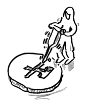
[[image:Define your structure directly.png|right|x200px|Define the structure directly on your sample]] | [[image:Define your structure directly.png|right|x200px|Define the structure directly on your sample]] | ||
By direct structure definition we mean that you form the structures for you device directly in the material that the device consist of without any masking steps. | By direct structure definition we mean that you form the structures for you device directly in the material that the device consist of without any masking steps. Some of the techniques may require a master. | ||
== Choose method of structuring/equipment == | == Choose method of structuring/equipment == | ||
| Line 23: | Line 13: | ||
* [[Specific Process Knowledge/Lithography/NanoImprintLithography|Nano Imprint Lithography]] | * [[Specific Process Knowledge/Lithography/NanoImprintLithography|Nano Imprint Lithography]] | ||
* [[Specific Process Knowledge/Back-end processing/Laser Micromachining Tool|Laser Micromachining Tool/ablation]] | * [[Specific Process Knowledge/Back-end processing/Laser Micromachining Tool|Laser Micromachining Tool/ablation]] | ||
* Dicing saw | * [[Specific Process Knowledge/Back-end processing/Disco Saw|Dicing saw]] | ||
== Materials for structuring == | == Materials for structuring == | ||
| Line 43: | Line 33: | ||
*Glass | *Glass | ||
**[[Specific Process Knowledge/Back-end processing/Laser Micromachining Tool|Laser ablation]] | **[[Specific Process Knowledge/Back-end processing/Laser Micromachining Tool|Laser ablation]] | ||
** | ** [[Specific Process Knowledge/Back-end processing/Disco Saw|Dicing saw]] | ||
**[[/Sandblasting|Sandblasting (at DTU Nanotech).]] | **[[Specific Process Knowledge/Back-end processing/Sandblasting|Sandblasting (at DTU Nanotech).]] | ||
== Comparison of equipment/material == | == Comparison of equipment/material == | ||
Revision as of 14:05, 6 October 2014
Feedback to this page: click here

Direct Structure Definiton

By direct structure definition we mean that you form the structures for you device directly in the material that the device consist of without any masking steps. Some of the techniques may require a master.
Choose method of structuring/equipment
- 2-Photon Polymerization Lithography
- Polymer Injection Molder
- Nano Imprint Lithography
- Laser Micromachining Tool/ablation
- Dicing saw
Materials for structuring
- Polymers
- Metals/Silicon/Graphene
- Glass
Comparison of equipment/material
- prøveformat/størrelse
- forudsætninger
- mønsterdannelse
- throughput
- min/max featuresize
- min/max aspect-ratio
- post-treatment
- degree of freedom
| Polymers | Nano Imprint Lithography | 2-Photon Polymerization Lithography | Polymer Injection Molder | Laser Micromachining Tool |
|---|---|---|---|---|
| Generel description | Low Pressure Chemical Vapour Deposition (LPCVD furnace process) | Plasma Enhanced Chemical Vapour Deposition (PECVD process) | Reactive sputtering | |
| Allowed materials |
Processed wafers have to be RCA cleaned |
|
Any |
| Metals/Silicon/Glass | Nano Imprint Lithography | 2-Photon Polymerization Lithography | Polymer Injection Molder | Laser Micromachining Tool |
|---|---|---|---|---|
| Generel description | Low Pressure Chemical Vapour Deposition (LPCVD furnace process) | Plasma Enhanced Chemical Vapour Deposition (PECVD process) | Reactive sputtering | |
| Allowed materials |
Processed wafers have to be RCA cleaned |
|
Any |