Specific Process Knowledge/Lithography/EBeamLithography/JEOL 9500 User Guide

Purpose, location and technical specifications
Type and location of machine
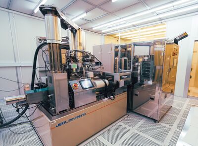
The JEOL JBX-9500FS electron beam lithography system is a spot electron beam lithography system designed for use in writing patterns (10 nm - 1 µm) in electron sensitive resists. The JEOL JBX-9500FS was purchased in 2012 and is installed in E-1 and E-2 at DTU Nanolab. The main console of the e-beam writer is installed in E-2 which is a class 10 (ISO 4) cleanroom with tight temperature and moisture control. The computer controlling the e-beam (EWS/9500) and the computer supporting the conversion of e-beam files are located in E-1 which is a class 100 (ISO 5) cleanroom.
Training and authorization
- Only authorized users are allowed to use this machine.
- In E-2, all users must keep within the area between the front side of the machine and the table with the pre-aligner setup. Only JEOL staff or DTU Nanolab staff may access the backside of the machine.
- No users, not even authorised users, are allowed to load a substrate into the automatic cassette transfer system.
- After your exposure, fully trained users can unload their cassettes from the automatic cassette transfer system and unmount their substrates.
- If you are unable to unmount your substrates before another user requires the cassette, you must accept that either the next user or DTU Nanolab personel unmount your substrates.
- Training can be requested by sending a mail with relevant process flow to training@nanolab.dtu.dk
Original JEOL Manual
The original JEOL manual for the e-beam writer JEOL JBX-9500FS is located on the O-drive: O:\CleanroomDrive\_Equipment\E-beam
Techical Specification
The system can be characterized as follows:
- The spot beam for electron beam writing is generated by a ZrO/W emitter and a four-stage electron beam focusing lens system.
- The maximum frequency of the deflector scanner is 100 MHz, i.e. the minimum beam dwell time is 10 ns.
- The acceleration voltage is locked at 100 kV.
- The e-beam writer can pattern structures with a minimum resolution of 10 nm.
- The maximum writing field size is 1000 µm x 1000 µm.
- The machine has cassettes that can contain either 6 wafers of 2” in size, 2 or 3 wafers of 4” in size, 1 wafer of 6” in size, 1 wafer of 8” in size, 4 chips of different sizes(slot sizes 4 mm, 8 mm, 12 mm, and 20 mm). See the Cassette specification page for more information
