Specific Process Knowledge/Lithography/EBeamLithography/eLINE: Difference between revisions
No edit summary |
|||
| (25 intermediate revisions by 2 users not shown) | |||
| Line 1: | Line 1: | ||
[[Image:eLINE-Plus.png|300x300px|right|]] | |||
<span style="background:#FF2800">THIS PAGE IS UNDER CONSTRUCTION</span>[[image:Under_construction.png|200px]] | <span style="background:#FF2800">THIS PAGE IS UNDER CONSTRUCTION</span>[[image:Under_construction.png|200px]] | ||
=Process information for the Raith eLINE Plus system= | =Process information for the Raith eLINE Plus system= | ||
The system was installed in the cleanroom in May 2022. As we get more familiar with the tool this page will be populated with relevant process information. | The system was installed in the cleanroom in May 2022. As we get more familiar with the tool this page will be populated with relevant process information. | ||
== System overview == | == System overview == | ||
The system is a dual use SEM and EBL exposure tool. For SEM applications the most notable difference from our other SEM's is the automation functionality that allows users to link a design to a substrate and simply | |||
[[File:RaithHolders.jpg|800px|thumb|right|4 inch wafer holder and 100 mm Universal Sample Holder (USH)]] | |||
The system is a dual use SEM and EBL exposure tool. For SEM applications the most notable difference from our other SEM's is the automation functionality that allows users to link a design to a substrate and simply from the design define areas to image and the tool will then image those areas without further user input. Once an imaging routine has been setup several hundred images can be acquired per hour. For a brief introduction to this feature see more [https://youtu.be/YoZF_6FeVb4 in this video.] | |||
| Line 15: | Line 24: | ||
==Dose information== | |||
[[Image:eLINE-Areas.png|800x800px|right|thumb|Base doses for exposure must be defined in the Pattern Parameter Calculation window.]] | [[Image:eLINE-Areas.png|800x800px|right|thumb|Base doses for exposure must be defined in the Pattern Parameter Calculation window.]] | ||
| Line 44: | Line 53: | ||
We recommend all EBL users to do a dose test prior to exposing samples of significant value. As a starting point you can consider to use the Demo.csf provided on the tool. This pattern is available in the auto generated user folder. The pattern consist of areas, curved elements, lines and dots as shown below. | We recommend all EBL users to do a dose test prior to exposing samples of significant value. As a starting point you can consider to use the Demo.csf provided on the tool. This pattern is available in the auto generated user folder. The pattern consist of areas, curved elements, lines and dots as shown below. Notice that several elements of the design are dose modulated, i.e. they can cover a range of doses in a single exposure. | ||
[[Image:DoseChip6.png|300x300px|right|thumb|Overview image of the dose test design provided on the tool.]] | [[Image:DoseChip6.png|300x300px|right|thumb|Overview image of the dose test design provided on the tool.]] | ||
===Table of dose to clear (area or curved elements) on Si substrate=== | ===Table of dose to clear (area or curved elements) on Si substrate=== | ||
The following table is merely at guideline to as to what sort of dose requirements to expect. Actual dose for your design will depend on substrate type and material, resist thickness, acceleration voltage, pattern density (proximity effects) and several other factors and thus users should always do a dose test with their actual pattern. Be aware that AR-N 8200 is in particular very dependent on PEB processing parameters. Refer to [[Specific_Process_Knowledge/Lithography/ARN8200|AR-N 8200 page]] for more information. | The following table is merely at guideline to as to what sort of dose requirements to expect. Actual dose for your design will depend on substrate type and material, resist thickness, acceleration voltage, pattern density (proximity effects) and several other factors and thus users should always do a dose test with their actual pattern. Be aware that AR-N 8200 is in particular very dependent on PEB processing parameters. Refer to [[Specific_Process_Knowledge/Lithography/ARN8200|AR-N 8200 page]] for more information. | ||
{| border="2" cellspacing="1" cellpadding="1" align="center" | {| border="2" cellspacing="1" cellpadding="1" align="center" | ||
! style="background:silver; color:black" colspan="4" | | ! style="background:silver; color:black" colspan="4" | Area dose [µC/cm2] | ||
|- valign="top" | |- valign="top" | ||
! style="background:silver; color:black" | Acc. voltage | ! style="background:silver; color:black" | Acc. voltage | ||
| Line 75: | Line 86: | ||
| style="background:lightgrey; color:black" | 180 | | style="background:lightgrey; color:black" | 180 | ||
|} | |} | ||
==Typical beam currents== | ==Typical beam currents== | ||
Beam current is a function of acceleration voltage and aperture and thus beam current is locked by the choice of acceleration voltage and aperture. Typical beam currents are given in the table below. The High Current (HC) mode can be activated in the Column Control panel. | |||
The High Current (HC) mode can be activated in the Column Control panel. | |||
| Line 156: | Line 160: | ||
|} | |} | ||
== | |||
Writefield dimension is a trade off between beam shot precision and field stitching. The maximum writefield size is 1000x1000 µm. The beam controller has a limit of | Writing time can be estimated in the software once a job is defined, it is however straight forward to estimate in advance based on area to pattern, A, dose to clear, d0, and beam current, I as: | ||
T = d0*A/I | |||
Notice that this estimate is only the beam dwell time and does not account for beam settling time or stage movement time. Typically process times are 3-4 times higher than the dwell time estimate but this will vary with pattern and writing conditions. | |||
==Writefields== | |||
[[Image:WF_imagescan.png|500x500px|right|thumb|WF alignment by image scan.]] | |||
[[Image:WF_linescan.png|500x500px|right|thumb|WF alignment by line scan.]] | |||
Writefield (WF) dimension is a trade off between beam shot precision and field stitching. The maximum writefield size is 1000x1000 µm. The beam controller has a limit of 50k addressable positions along each axis and hence for a 1000x1000 µm writefield the minimum beam position grid (pitch) is 20 nm. For a 100x100 µm writefield the minimum beam pitch is 2 nm. Thus the precision is higher for smaller writing fields. Smaller writing fields will however fracture a design into more fields and create more field boundaries with higher potential for stitching errors. | |||
To minimize stitching errors it is important to perform WF alignment before writing. WF alignment should be done on either a particle or an existing feature close to the writing area. WF alignment can be done in three different ways: | |||
:1. Manual alignment by image scan to a particle or feature | |||
:2. Automatic alignment by image scan of a particle or feature | |||
:3. Automatic alignment by line scan of feature (preferably a cross) | |||
The concept is illustrated in the two drawings and relies on the high precision of the laser interferometer driven stage (about 1 nm precision). When using image scan for WF alignment the user must center the chosen feature or particle in the image field. When executing the WF alignment the stage will displace a bit less than half a WF in one direction. The beam will then deflect back by the same amount and make an image scan. If the WF is perfectly aligned the deflected image will be show the feature in the center of the image. In manual alignment mode the user will indicate any offset, in automatic mode the system will do image analysis and determine the offset. For WF alignment 3-8 different stage positions will be scanned in this way and at the end a correction is calculated and applied. | |||
WF alignment can also be done by line scanning, preferably over a cross from a previous lithography step. The procedure is the same as above except that at each position instead of making an image scan the system makes two line scans and detects each leg of the cross to calculate the center of the cross and in turn the offset of the cross. Again this is done for 3-8 different positions. | |||
Latest revision as of 12:02, 8 May 2023
THIS PAGE IS UNDER CONSTRUCTION
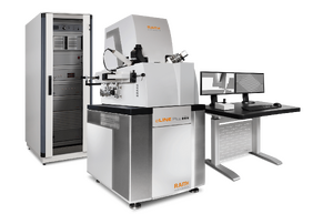
Process information for the Raith eLINE Plus system
The system was installed in the cleanroom in May 2022. As we get more familiar with the tool this page will be populated with relevant process information.
System overview
The system is a dual use SEM and EBL exposure tool. For SEM applications the most notable difference from our other SEM's is the automation functionality that allows users to link a design to a substrate and simply from the design define areas to image and the tool will then image those areas without further user input. Once an imaging routine has been setup several hundred images can be acquired per hour. For a brief introduction to this feature see more in this video.
For EBL the system is a variable voltage exposure tool with a maximum acceleration voltage of 30 kV and beam currents from 0.01 to 12.6 nA. The stage position is controlled by a laser interferometer and has a position accuracy of about 1 nm.
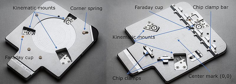
Currently two holders are available, a 4" wafer holder and a 100 mm Universal Sample Holder (USH) for substrates up to about 75x75 mm. Chips can be clamped on either of the 8 chip clamps on the USH. The sample holders will rest on three ceramic balls on the stage, each ceramic ball fits into one of the kinematic mounts of the sample holder. The kinematic mounts are adjusted to keep the sample holder as level as possible. When handling the sample holders it is important not to touch the kinematic mounts.
Dose information
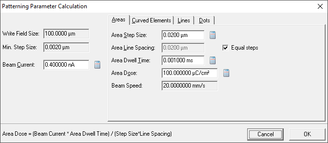
The eLINE tool operates with four different design element types; area, curved elements, line and dot. The element types are classified as:
- Area: Polygons
- Curved elements: Elements that have an adjustable radius
- Line: Zero-width line
- Dot: Single point/vertice element
The software allows the user to define different doses for the four different types of elements and thus it is essential to know how the design is drawn and interpreted. The units used are:
- Area dose [µC/cm2],
- Curved element dose [µC/cm2]
- Line dose [pC/cm]
- Dot dose [pC].
Also notice that the unit prefix changes from micro to pico. We recommend setting the same dose for area and curved elements.
The dose for each type can be setup under the "Patterning Parameter". Before updating the requested dose the beam current must be measured from the "Patterning Parameter" page. In all tabs the user will set a step size, i.e. the distance between beam positions and a dose. The dwell time must then be updated by clicking the calculate icon next to the dwell time field. The dwell time will be calculated based on the last beam current measurement.
Dot dose, line dose and curved element doses can be disabled in the Patterning Parameter window and in that case the system will IGNORE the type of elements that are disabled, i.e. they will not be written.
We recommend all EBL users to do a dose test prior to exposing samples of significant value. As a starting point you can consider to use the Demo.csf provided on the tool. This pattern is available in the auto generated user folder. The pattern consist of areas, curved elements, lines and dots as shown below. Notice that several elements of the design are dose modulated, i.e. they can cover a range of doses in a single exposure.
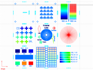
Table of dose to clear (area or curved elements) on Si substrate
The following table is merely at guideline to as to what sort of dose requirements to expect. Actual dose for your design will depend on substrate type and material, resist thickness, acceleration voltage, pattern density (proximity effects) and several other factors and thus users should always do a dose test with their actual pattern. Be aware that AR-N 8200 is in particular very dependent on PEB processing parameters. Refer to AR-N 8200 page for more information.
| Area dose [µC/cm2] | |||
|---|---|---|---|
| Acc. voltage | AR-P 6200.09 (180 nm) | PMMA 950k | AR-N 8200.06 |
| 10 kV | 30 | - | - |
| 20 kV | 70 | - | - |
| 30 kV | 100 | - | 180 |
Typical beam currents
Beam current is a function of acceleration voltage and aperture and thus beam current is locked by the choice of acceleration voltage and aperture. Typical beam currents are given in the table below. The High Current (HC) mode can be activated in the Column Control panel.
| Typical beam current [nA] as function of acceleration voltage and aperture | |||||||
|---|---|---|---|---|---|---|---|
| Acc. voltage / Aperture | 7 µm | 10 µm | 15 µm | 20 µm | 30 µm | 60 µm | 120 µm |
| 10 kV | 0.01 | 0.02 | 0.06 | 0.10 | 0.23 | 0.99 | 3.87 |
| 10 kV HC | 0.02 | 0.05 | 0.12 | 0.20 | 0.39 | 1.96 | 7.67 |
| 20 kV | 0.02 | 0.04 | 0.09 | 0.16 | 0.36 | 1.53 | 6.06 |
| 20 kV HC | 0.03 | 0.08 | 0.18 | 0.32 | 0.61 | 3.03 | 11.9 |
| 30 kV | 0.02 | 0.04 | 0.10 | 0.17 | 0.38 | 1.65 | 6.53 |
| 30 kV HC | 0.04 | 0.09 | 0.19 | 0.34 | 0.64 | 3.20 | 12.6 |
Writing time can be estimated in the software once a job is defined, it is however straight forward to estimate in advance based on area to pattern, A, dose to clear, d0, and beam current, I as:
T = d0*A/I
Notice that this estimate is only the beam dwell time and does not account for beam settling time or stage movement time. Typically process times are 3-4 times higher than the dwell time estimate but this will vary with pattern and writing conditions.
Writefields
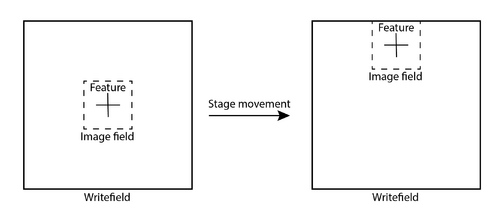
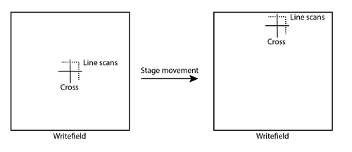
Writefield (WF) dimension is a trade off between beam shot precision and field stitching. The maximum writefield size is 1000x1000 µm. The beam controller has a limit of 50k addressable positions along each axis and hence for a 1000x1000 µm writefield the minimum beam position grid (pitch) is 20 nm. For a 100x100 µm writefield the minimum beam pitch is 2 nm. Thus the precision is higher for smaller writing fields. Smaller writing fields will however fracture a design into more fields and create more field boundaries with higher potential for stitching errors.
To minimize stitching errors it is important to perform WF alignment before writing. WF alignment should be done on either a particle or an existing feature close to the writing area. WF alignment can be done in three different ways:
- 1. Manual alignment by image scan to a particle or feature
- 2. Automatic alignment by image scan of a particle or feature
- 3. Automatic alignment by line scan of feature (preferably a cross)
The concept is illustrated in the two drawings and relies on the high precision of the laser interferometer driven stage (about 1 nm precision). When using image scan for WF alignment the user must center the chosen feature or particle in the image field. When executing the WF alignment the stage will displace a bit less than half a WF in one direction. The beam will then deflect back by the same amount and make an image scan. If the WF is perfectly aligned the deflected image will be show the feature in the center of the image. In manual alignment mode the user will indicate any offset, in automatic mode the system will do image analysis and determine the offset. For WF alignment 3-8 different stage positions will be scanned in this way and at the end a correction is calculated and applied.
WF alignment can also be done by line scanning, preferably over a cross from a previous lithography step. The procedure is the same as above except that at each position instead of making an image scan the system makes two line scans and detects each leg of the cross to calculate the center of the cross and in turn the offset of the cross. Again this is done for 3-8 different positions.
