Specific Process Knowledge/Thermal Process/Oxidation/Breakdown voltage measurements: Difference between revisions
No edit summary |
No edit summary |
||
| (20 intermediate revisions by 2 users not shown) | |||
| Line 1: | Line 1: | ||
'''Feedback to this page''': '''[mailto:labadviser@nanolab.dtu.dk?Subject=Feed%20back%20from%20page%20http://labadviser.nanolab.dtu.dk/index.php/Specific_Process_Knowledge/Thermal_Process/Oxidation/Breakdown_voltage_measurementsM click here]''' | |||
<i> Unless otherwise stated, this page is written by <b>DTU Nanolab internal</b></i> | |||
=Breakdown voltage measurements= | |||
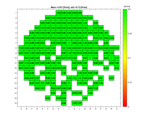
In order to evaluate the quality of the wet and dry oxide layers that can be grown in the A1 Boron Drive-in and Pre-dep and the A3 Phosphorus Pre-dep furnaces, some breakdown voltage measurement have been made. The breakdown voltage is the maximum voltage that can be applied to an insulating material like silicon oxide, before it starts to conduct. | |||
The breakdown voltage measurements were performed using a automated measure setup at DTU Health Tech. This setup automatically measures the breakdown voltage in a pattern over each wafer. Each field in the pattern has a gold contact. The measurements are done by applying an increasing reverse voltage to each field in the pattern via a probe, until certain current is reached that indicates a breakdown, see the drawing. | |||
The measurements were made in November 2021. | <!--[[image:Breakdown.jpg|850px]]--> | ||
Some fields in pattern are excluded from the results. The reason for this is either that the contact between the probe and the gold contact has not been been sufficient, or the probe has become dirty during the measurement. | |||
The absolute breakdown voltage has been measured, and the relative breakdown voltage has been calculated. The relative breakdown voltage is the breakdown voltage per nm of the oxide layer. | |||
<i>The measurements were made in November 2021 with help from Kitty Steenberg and Rune Sixten Grass from DTU Health Tech.</i> | |||
| Line 17: | Line 24: | ||
The procedure for the breakdown voltage measurements is the following: | The procedure for the breakdown voltage measurements is the following: | ||
* RCA clean new wafers | |||
* Grow wet or dry oxide in the A1 or A3 furnace | * RCA clean new Si wafers (double side polished wafers from the box TP473) | ||
* Spin resist on the front of the wafers | * Grow wet or dry oxide of both sides of the wafers in the A1 or A3 furnace | ||
* Remove the oxide on the | * Spin resist on the front side of the wafers | ||
* Remove the resist on the front of the wafers using plasma ashing | * Remove the oxide on the back side of the wafers using BHF in Oxide etch 2 | ||
* Deposit 10 nm Ti and 100 nm Au through a shadow mask using e-beam deposition in the Temescal | * Remove the resist on the front side of the wafers using plasma ashing | ||
* Deposit 10 nm Ti and 100 nm Au through a shadow mask on the front side of the wafers using e-beam deposition in the Temescal | |||
* Measure the break-down voltage | * Measure the break-down voltage | ||
==Breakdown voltage results for the A1 Boron Drive-in and Pre-dep furnace== | ==Breakdown voltage results for the A1 Boron Drive-in and Pre-dep furnace== | ||
| Line 57: | Line 66: | ||
</gallery> | </gallery> | ||
<i>The measurements were made in November 2021 with help from Kitty Steenberg and Rune Sixten Grass from DTU Health Tech.</i> | |||
==Breakdown voltage results for the A2 Gate Oxide furnace== | |||
===Breakdown voltage measurements for dry oxide=== | |||
Oxidation parameters: | |||
*Temperature: 1050 C | |||
*Oxidation time: 1 h 40 min | |||
*Annealing time: 20 min | |||
Oxide thickness: ~150 nm | |||
<gallery caption="A2 furnace, dry oxidation" widths="600px" heights="400px" perrow="2"> | |||
image:2022-02-08_10-56-57_Wafer_A2_150nm_Abs.png|'''Absolute breakdown voltage''' | |||
image:2022-02-08_10-56-57_Wafer_A2_150nm_Rel.png|'''Relative breakdown voltage''' | |||
</gallery> | |||
The | <i>The measurements were made in February 2022 with help from Kitty Steenberg and Rune Sixten Grass from DTU Health Tech.</i> | ||
==Breakdown voltage results for the A3 Phosphorus Drive-in furnace== | ==Breakdown voltage results for the A3 Phosphorus Drive-in furnace== | ||
| Line 79: | Line 106: | ||
image:2021-11-09_08-27-49_Wafer_A3_DRY1050_118nm_Rel.jpg|'''Relative breakdown voltage''' | image:2021-11-09_08-27-49_Wafer_A3_DRY1050_118nm_Rel.jpg|'''Relative breakdown voltage''' | ||
</gallery> | </gallery> | ||
===Breakdown voltage measurements for wet oxide=== | ===Breakdown voltage measurements for wet oxide=== | ||
| Line 96: | Line 122: | ||
</gallery> | </gallery> | ||
<i>The measurements were made in November 2021 with help from Kitty Steenberg and Rune Sixten Grass from DTU Health Tech.</i> | |||
==Breakdown voltage results for Oxidation (8") furnace (E1)== | |||
===Breakdown voltage measurements for dry oxide=== | |||
Oxidation parameters: | |||
*Temperature: 1050 C | |||
*Oxidation time: 1 h 40 min | |||
*Annealing time: 20 min | |||
Oxide thickness: ~117 nm | |||
<gallery caption="E1 furnace, dry oxidation" widths="600px" heights="400px" perrow="2"> | |||
image:2022-02-08_10-47-35_Wafer_E1_117nm_Abs.png|'''Absolute breakdown voltage''' | |||
image:2022-02-08_10-47-35_Wafer_E1_117nm_Rel.png|'''Relative breakdown voltage''' | |||
</gallery> | |||
The | <i>The measurements were made in February 2022 with help from Kitty Steenberg and Rune Sixten Grass from DTU Health Tech.</i> | ||
Latest revision as of 10:43, 15 June 2023
Feedback to this page: click here
Unless otherwise stated, this page is written by DTU Nanolab internal
Breakdown voltage measurements
In order to evaluate the quality of the wet and dry oxide layers that can be grown in the A1 Boron Drive-in and Pre-dep and the A3 Phosphorus Pre-dep furnaces, some breakdown voltage measurement have been made. The breakdown voltage is the maximum voltage that can be applied to an insulating material like silicon oxide, before it starts to conduct.
The breakdown voltage measurements were performed using a automated measure setup at DTU Health Tech. This setup automatically measures the breakdown voltage in a pattern over each wafer. Each field in the pattern has a gold contact. The measurements are done by applying an increasing reverse voltage to each field in the pattern via a probe, until certain current is reached that indicates a breakdown, see the drawing.
Some fields in pattern are excluded from the results. The reason for this is either that the contact between the probe and the gold contact has not been been sufficient, or the probe has become dirty during the measurement.
The absolute breakdown voltage has been measured, and the relative breakdown voltage has been calculated. The relative breakdown voltage is the breakdown voltage per nm of the oxide layer.
The measurements were made in November 2021 with help from Kitty Steenberg and Rune Sixten Grass from DTU Health Tech.
Procedure
The procedure for the breakdown voltage measurements is the following:
- RCA clean new Si wafers (double side polished wafers from the box TP473)
- Grow wet or dry oxide of both sides of the wafers in the A1 or A3 furnace
- Spin resist on the front side of the wafers
- Remove the oxide on the back side of the wafers using BHF in Oxide etch 2
- Remove the resist on the front side of the wafers using plasma ashing
- Deposit 10 nm Ti and 100 nm Au through a shadow mask on the front side of the wafers using e-beam deposition in the Temescal
- Measure the break-down voltage
Breakdown voltage results for the A1 Boron Drive-in and Pre-dep furnace
Breakdown voltage measurements for dry oxide
Oxidation parameters:
- Temperature: 1050 C
- Oxidation time: 1 h 40 min
- Annealing time: 20 min
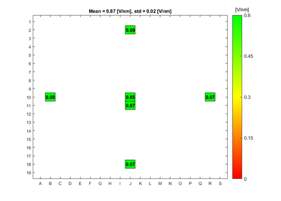
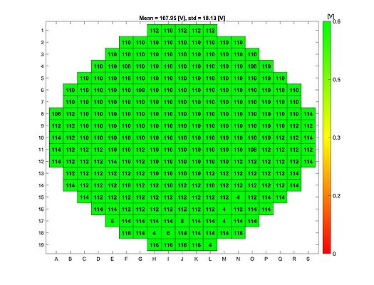
Oxide thickness: ~100 nm
- A1 furnace, dry oxidation
Absolute breakdown voltage
Relative breakdown voltage


Breakdown voltage measurements for wet oxide
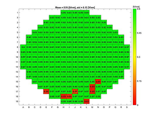
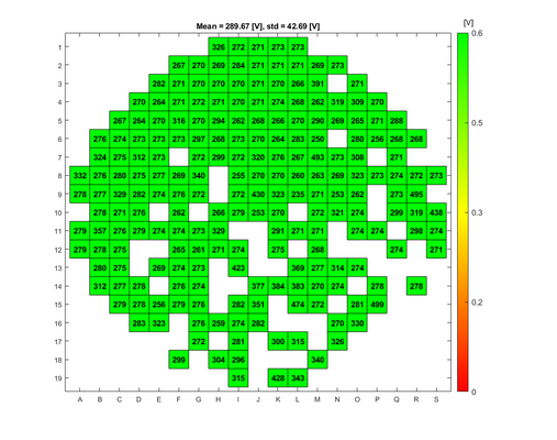
Oxidation parameters:
- Temperature: 1050 C
- Oxidation time: 30 min
- Annealing time: 20 min
Oxide thickness: ~300 nm
- A1 furnace, wet oxidation
Absolute breakdown voltage
Relative breakdown voltage


The measurements were made in November 2021 with help from Kitty Steenberg and Rune Sixten Grass from DTU Health Tech.
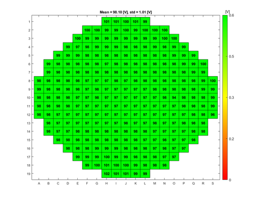
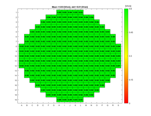
Breakdown voltage results for the A2 Gate Oxide furnace
Breakdown voltage measurements for dry oxide
Oxidation parameters:
- Temperature: 1050 C
- Oxidation time: 1 h 40 min
- Annealing time: 20 min
Oxide thickness: ~150 nm
- A2 furnace, dry oxidation

Absolute breakdown voltage
Relative breakdown voltage


The measurements were made in February 2022 with help from Kitty Steenberg and Rune Sixten Grass from DTU Health Tech.
Breakdown voltage results for the A3 Phosphorus Drive-in furnace
Right before the breakdown voltage measurements were made, all quartz parts in the furnace were changed.
Breakdown voltage measurements for dry oxide
Oxidation parameters:
- Temperature: 1050 C
- Oxidation time: 1 h 40 min
- Annealing time: 20 min
Oxide thickness: ~110 nm
- A3 furnace, dry oxidation
Absolute breakdown voltage
Relative breakdown voltage


Breakdown voltage measurements for wet oxide
Oxidation parameters:
- Temperature: 1050 C
- Oxidation time: 30 min
- Annealing time: 20 min
Oxide thickness: ~320 nm
- A3 furnace, wet oxidation
Absolute breakdown voltage
Relative breakdown voltage


The measurements were made in November 2021 with help from Kitty Steenberg and Rune Sixten Grass from DTU Health Tech.
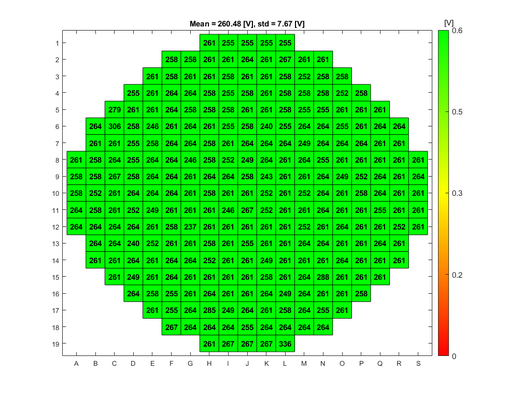
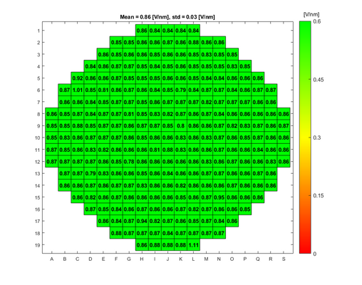
Breakdown voltage results for Oxidation (8") furnace (E1)
Breakdown voltage measurements for dry oxide
Oxidation parameters:
- Temperature: 1050 C
- Oxidation time: 1 h 40 min
- Annealing time: 20 min
Oxide thickness: ~117 nm
- E1 furnace, dry oxidation
Absolute breakdown voltage

Relative breakdown voltage


The measurements were made in February 2022 with help from Kitty Steenberg and Rune Sixten Grass from DTU Health Tech.