Specific Process Knowledge/Thermal Process/C1 Furnace Anneal-oxide: Difference between revisions
| Line 64: | Line 64: | ||
*Silicon wafers with layers of silicon oxide or silicon (oxy)nitride (RCA cleaned) | *Silicon wafers with layers of silicon oxide or silicon (oxy)nitride (RCA cleaned) | ||
*Wafers from the LPCVD furnaces | *Wafers from the LPCVD furnaces | ||
*Wafers from | *Wafers from PECVD4 | ||
|- | |- | ||
|} | |} | ||
Revision as of 09:37, 30 August 2017
Feedback to this page: click here
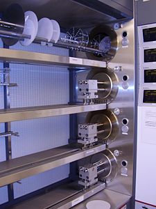
Anneal-oxide furnace (C1)
The Anneal-oxide furnace (C1) is a Tempress horizontal furnace for oxidation and annealing of silicon wafers, e.g with layers of oxide, polysilicon or BPSG glass (from PECVD2). Both 100 mm and 150 mm wafers can be processed in the furnace.
The Anneal-oxide furnace is the top furnace tube in the C-stack furnaces, which positioned in cleanroom B-1. Most of wafers have to do RCA cleaned before they enter the furnace. The only exceptions are the brand new wafers, the wafers from A-stack furnaces, the wafers from PECVD4 and the LPCVD furnaces. Please check the cross contamination information in LabManager before you use the furnace
The user manual, technical information and contact information can be found in LabManager:
Process knowledge
- WET oxidation: with steamer
- DRY oxidation: look at the Oxidation page
- Annealing: look at the Annealing page
| Purpose |
|
Oxidation:
|
|---|---|---|
| Performance | Film thickness |
|
| Process parameter range | Process Temperature |
|
| Process pressure |
| |
| Gas flows |
| |
| Substrates | Batch size |
|
| Substrate materials allowed |
|
