Specific Process Knowledge/Imprinting
The contents on this page, including all images and pictures, was created by DTU Nanolab staff unless otherwise stated.
Feedback to this page: click here
Imprinting
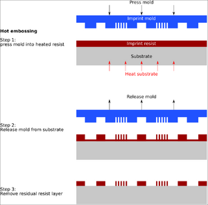
Imprinting (hot embossing) is a parallel transfer of a pattern made by a serial technique (often e-beam). First a stamp is made, usually in Si or SiO however other materials could also be used. The pattern on the stamp is then transferred to a polymer (on a different substrate), by heating both stamp and substrate to above the glass transition temperature T of the polymer and then pressing the stamp and the substrate together, hence deforming the polymer on the substrate. The stamp and substrate are then cooled down and only separated when the temperature is well below T of the polymer. Normally the stack is often cooled to room temperature to easily separate the two parts.
After the stamp has been removed it is possible to use the polymer as e.g. an etch mask in a dry etch to transfer the patters from the stamp to the substrate.
It is necessary to deposit anti stiction coating on the stamp to ensure that it can be separated from the substrate, this is done in either the MVD or the ASE. If the stamp it not anti stiction coated it is likely that either (or both) the stamp and substrate will break during separation. It is only necessary to deposit anti stiction coating on the stamp one time even though it is used a multiple of times.
Stamp for imprint
A stamp for imprint lithography is usually made in Si or SiO, however other materials could also be used. Here is a process flow for stamp made of SU8 resist. Stamp fabrication flow.
Imprint resist
Imprint Resist Overview
Here is a table with 2 different imprint resists we have recently used in the cleanroom, with links to a purchase manufactor, technical reports about resist properties and a current process flow, tested in our cleanroom.
| Resist | Manufacturer | Comments | Technical reports | Thinner | Spinner | Rinse | Process flows (in docx-format) |
| Topas | micro resist technology | Users may purchase own resist. | Topas.pdf | LabSpin03 or LabSpin03 | IPA | ||
| mr-I 7030R | micro resist technology | We purchase only mr-I 7030R, for use it please contact Lithography. | mr-I 7030R.pdf | mr-T 1050 | LabSpin03 or LabSpin03 | Acetone | Preparation substrate with mr-I 7030R: Preparation substrate with imprint layer |
Imprinting parameters
When you do an imprint you may consider 3 most important parameters: pressure, temperature and imprinting time. All those parameters are depending of printable resists molecular weight and its glas transition temperature.
Choose an equipment
- MVD - Molecular Vapor Deposition - Antistiction coater for silicon stamps
- Drop Shape Analyzer - Tool to measure the hydrophobicity of the antistiction layer
- Imprinter 01 - Tool to imprint


